LTC1250 - Very Low Noise Zero-Drift Bridge Amplifier
The LTC1250 incorporates an improved output stage capable of driving 4.3V into a 1k load with a single 5V supply; it will swing ±4.9V into 5k with ±5V supplies. The input common mode range includes ground with single power supply voltages above 12V. Supply current is 3mA with a ±5V supply, and overload recovery times from positive and negative saturation are 0.5ms and 1.5ms, respectively. The internal nulling clock is set at 5kHz for optimum low frequency noise and offset drift; no external connections are necessary.
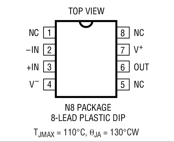
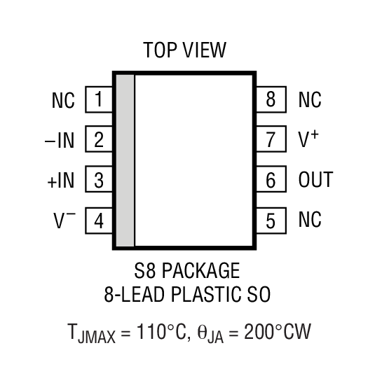
The LTC1250 is available in a standard 8-pin plastic DIP and 8-pin SO packages.
Protected by U.S. Patents including 4933642.
| Part Number | Package | Temp | Price(1-99) | Price (1k)* |
|---|---|---|---|---|
| LTC1250CN8#PBF | N-8 | C | $3.70 | $2.85 |
| LTC1250CS8#PBF | SO-8 | C | $4.20 | $3.25 |
| LTC1250CS8#TRPBF | SO-8 | C | $3.31 |
Demo Boards
| Part Number | Description | Price |
|---|---|---|
| DC417B | DIP8, MS8, S8, SOT23-6 | Multi-Footprint General Purpose Board for Single Op. Amp | $25.00 |


