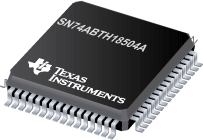
SN74ABTH18504A 具有 20 位通用总线收发器的扫描测试设备
 The 'ABTH18504A and 'ABTH182504A scan test devices with 20-bit universal bus transceivers are members of the Texas Instruments SCOPETM testability integrated-circuit family. This family of devices supports IEEE Standard 1149.1-1990 boundary scan to facilitate testing of complex circuit-board assemblies. Scan access to the test circuitry is accomplished via the 4-wire test access port (TAP) interface.
In the normal mode, these devices are 20-bit universal bus transceivers that combine D-type latches and D-type flip-flops to allow data flow in transparent, latched, or clocked modes. The test circuitry can be activated by the TAP to take snapshot samples of the data appearing at the device pins or to perform a self test on the boundary-test cells.
|
SN74ABTH18504A |
| Voltage Nodes(V) |
5 |
| Vcc range(V) |
4.5 to 5.5 |
| Input Level |
TTL |
| Logic |
True |
| No. of Outputs |
20 |
| Output Drive(mA) |
-32/64 |
| tpd max(ns) |
5.5 |
| Output Level |
TTL |
| Static Current |
14.6 |
| Rating |
Catalog |
| Technology Family |
ABT |
SN74ABTH18504A 特性
- Members of the Texas Instruments SCOPETM Family of Testability Products
- Members of the Texas Instruments WidebusTM Family
- Compatible With the IEEE Standard 1149.1-1990 (JTAG) Test Access Port and Boundary-Scan Architecture
- UBT TM (Universal Bus Transceiver) Combines D-Type Latches and D-Type Flip-Flops for Operation in Transparent, Latched, or Clocked Mode
- Bus Hold on Data Inputs Eliminates the Need for External Pullup Resistors
- B-Port Outputs of 'ABTH182504A Devices Have Equivalent 25-
 Series Resistors, So No External Resistors Are Required
- State-of-the-Art EPIC-IIB TM BiCMOS Design
- One Boundary-Scan Cell Per I/O Architecture Improves Scan Efficiency
- SCOPE TM Instruction Set
- IEEE Standard 1149.1-1990 Required Instructions and Optional CLAMP and HIGHZ
- Parallel-Signature Analysis at Inputs
- Pseudo-Random Pattern Generation From Outputs
- Sample Inputs/Toggle Outputs
- Binary Count From Outputs
- Device Identification
- Even-Parity Opcodes
- Packaged in 64-Pin Plastic Thin Quad Flat (PM) Packages Using 0.5-mm Center-to-Center Spacings and 68-Pin Ceramic Quad Flat (HV) Packages Using 25-mil Center-to-Center Spacings
SN74ABTH18504A 芯片订购指南
| 器件 |
状态 |
温度 |
价格(美元) |
封装 | 引脚 |
封装数量 | 封装载体 |
丝印标记 |
| SN74ABTH18504APMG4 |
ACTIVE |
-40 to 85 |
16.70 | 1ku |
LQFP (PM) | 64 |
160 | JEDEC TRAY (10+1) |
|
| SN74ABTH18504APM |
ACTIVE |
-40 to 85 |
16.70 | 1ku |
LQFP (PM) | 64 |
160 | JEDEC TRAY (10+1) |
|
SN74ABTH18504A 质量与无铅数据
| 器件 |
环保计划* |
铅/焊球涂层 |
MSL 等级/回流焊峰 |
环保信息与无铅 (Pb-free) |
DPPM / MTBF / FIT 率 |
| SN74ABTH18504APMG4 |
Green (RoHS & no Sb/Br) |
CU NIPDAU |
Level-3-260C-168 HR |
SN74ABTH18504APMG4 |
SN74ABTH18504APMG4 |
| SN74ABTH18504APM |
Green (RoHS & no Sb/Br) |
CU NIPDAU |
Level-3-260C-168 HR |
SN74ABTH18504APM |
SN74ABTH18504APM |
SN74ABTH18504A 应用技术支持与电子电路设计开发资源下载
- SN74ABTH18504A 数据资料 dataSheet 下载.PDF
- TI 德州仪器特殊逻辑产品选型与价格 . xls
- Shelf-Life Evaluation of Lead-Free Component Finishes (PDF 1305 KB)
- Understanding and Interpreting Standard-Logic Data Sheets (PDF 857 KB)
- TI IBIS File Creation, Validation, and Distribution Processes (PDF 380 KB)
- Implications of Slow or Floating CMOS Inputs (PDF 101 KB)
- CMOS Power Consumption and CPD Calculation (PDF 89 KB)
- Designing With Logic (PDF 186 KB)
- Live Insertion (PDF 150 KB)
- Input and Output Characteristics of Digital Integrated Circuits (PDF 1708 KB)
- Using High Speed CMOS and Advanced CMOS in Systems With Multiple Vcc (PDF 43 KB)
- HiRel Unitrode Power Management Brochure (PDF 206 KB)
- LOGIC Pocket Data Book (PDF 6001 KB)
- HiRel Unitrode Power Management Brochure (PDF 206 KB)
- Logic Cross-Reference (PDF 2938 KB)
 The 'ABTH18504A and 'ABTH182504A scan test devices with 20-bit universal bus transceivers are members of the Texas Instruments SCOPETM testability integrated-circuit family. This family of devices supports IEEE Standard 1149.1-1990 boundary scan to facilitate testing of complex circuit-board assemblies. Scan access to the test circuitry is accomplished via the 4-wire test access port (TAP) interface.
 Series Resistors, So No External Resistors Are Required
