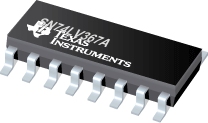
SN74LV367A 具有三态输出的六路缓冲器和线路驱动器

SN74LV367A 描述
The 'LV367A devices are hex buffers and line drivers designed for 2-V to 5.5-V VCC operation. These devices are designed specifically to improve both the performance and density of 3-state memory address drivers, clock drivers, and bus-oriented receivers and transmitters.
The 'LV367A devices are organized as dual 4-line and 2-line buffers/drivers with active-low output-enable (1OE\ and 2OE\) inputs. When OE\ is low, the device passes noninverted data from the A inputs to the Y outputs. When OE\ is high, the outputs are in the high-impedance state.
To ensure the high-impedance state during power up or power down, OE\ should be tied to VCC through a pullup resistor; the minimum value of the resistor is determined by the current-sinking capability of the driver
| SN74LV367A | |
| Voltage Nodes(V) | 5, 3.3, 2.5 |
| Vcc range(V) | 2.0 to 5.5 |
| Logic | True |
| Input Level | LVTTL |
| Output Level | LVTTL |
| Output Drive(mA) | -8/8 |
| No. of Outputs | 6 |
| tpd max(ns) | 10 |
| Static Current | 0.02 |
| Rating | Catalog |
| Technology Family | LV-A |
SN74LV367A 特性
- 2-V to 5.5-V VCC Operation
- Max tpd of 7 ns at 5 V
- Typical VOLP (Output Ground Bounce) <0.8 V at VCC = 3.3 V, TA = 25°C
- Typical VOHV (Output VOH Undershoot) >2.3 V at VCC = 3.3 V, TA = 25°C
- Support Mixed-Mode Voltage Operation on All Ports
- Latch-Up Performance Exceeds 100 mA Per JESD 78, Class II
- ESD Protection Exceeds JESD 22
- 2000-V Human-Body Model (A114-A)
- 200-V Machine Model (A115-A)
- 1000-V Charged-Device Model (C101)
SN74LV367A 芯片订购指南
| 器件 | 状态 | 温度 | 价格(美元) | 封装 | 引脚 | 封装数量 | 封装载体 | 丝印标记 |
| SN74LV367AD | ACTIVE | -40 to 85 | 0.28 | 1ku | SOIC (DW) | 16 | 40 | TUBE | LV367A |
| SN74LV367ADE4 | ACTIVE | -40 to 85 | 0.28 | 1ku | SOIC (DW) | 16 | 40 | TUBE | LV367A |
| SN74LV367ADG4 | ACTIVE | -40 to 85 | 0.28 | 1ku | SOIC (DW) | 16 | 40 | TUBE | LV367A |
SN74LV367A 质量与无铅数据
| 器件 | 环保计划* | 铅/焊球涂层 | MSL 等级/回流焊峰 | 环保信息与无铅 (Pb-free) | DPPM / MTBF / FIT 率 |
| SN74LV367AD | Green (RoHS & no Sb/Br) | CU NIPDAU | Level-1-260C-UNLIM | SN74LV367AD | SN74LV367AD |
| SN74LV367ADE4 | Green (RoHS & no Sb/Br) | CU NIPDAU | Level-1-260C-UNLIM | SN74LV367ADE4 | SN74LV367ADE4 |
| SN74LV367ADG4 | Green (RoHS & no Sb/Br) | CU NIPDAU | Level-1-260C-UNLIM | SN74LV367ADG4 | SN74LV367ADG4 |
SN74LV367A 应用技术支持与电子电路设计开发资源下载
- SN74LV367A 数据资料 dataSheet 下载.PDF
- TI 德州仪器缓冲器、驱动器/收发器产品选型与价格 . xls
- CMOS 非缓冲反向器在振荡器电路中的使用 (PDF 951 KB)
- Semiconductor Packing Methodology (PDF 3005 KB)
- 逻辑产品选择指南 2006/2007 (修订版 Z)(4462KB)
- 标准线性和逻辑产品 5 分钟指南 (786KB)
- 了解和解释标准逻辑数据表
- LOGIC Pocket Data Book (PDF 6001 KB)
- HiRel Unitrode Power Management Brochure (PDF 206 KB)
- Logic Cross-Reference (PDF 2938 KB)
