74LVC1G34:单门
| Part Number | Data Sheet | SPICE Model | Number of Gates | Family | VCC Min (V) | VCC Max (V) | tpd max @ (1.5V) (ns) | tpd max @ (1.8V) (ns) | tpd max @ (2.5V) (ns) | tpd max @ (3.3V) (ns) | tpd max @ (5.0V) (ns) | Output Current |
|---|---|---|---|---|---|---|---|---|---|---|---|---|
| 74LVC1G34 | 74LVC1G34.pdf | - | 1 | LVC | 1.65 | 5.5 | - | 7.5 | 5 | 4.2 | 3.7 | 32 |
Description
The 74LVC1G34 is a single buffer gate with a standard push-pull output. The device is designed for operation with a power supply range of 1.65V to 5.5V. The inputs are tolerant to 5.5V allowing this device to be used in a mixed voltage environment. The device is fully specified for partial power down applications using IOFF. The IOFF circuitry disables the output preventing damaging current backflow when the device is powered down.
Application
- Voltage Level Shifting
- General Purpose Logic
- Power Down Signal Isolation
- Wide array of products such as: - PCs, Networking, Notebooks, Netbooks, PDAs - Tablet Computers, E-readers - Computer Peripherals, Hard Drives, CD/DVD ROM - TV, DVD, DVR, Set Top Box - Cell Phones, Personal Navigation / GPS - MP3 players ,Cameras, Video Recorders
Features
- Wide Supply Voltage Range from 1.65 to 5.5V
- ± 24mA Output Drive at 3.3V
- CMOS low power consumption
- IOFF Supports Partial-Power-Down Mode Operation
- Inputs accept up to 5.5V
- ESD Protection Tested per JESD 22
- Exceeds 200-V Machine Model (A115-A)
- Exceeds 2000-V Human Body Model (A114-A)
- Exceeds 1000-V Charged Device Model (C101C)
- Latch-Up Exceeds 100mA per JESD 78, Class II
- Range of Package Options
- Direct Interface with TTL Levels
- Totally Lead-Free & Fully RoHS Compliant
- Halogen and Antimony Free. “Green” Device
订购型号
- 74LVC1G34FS3-7
- 74LVC1G34FW4-7
- 74LVC1G34FW5-7
- 74LVC1G34FX4-7
- 74LVC1G34FZ4-7
- 74LVC1G34SE-7
- 74LVC1G34W5-7
- 74LVC1G34Z-7
SOT25

SOT353

SOT553

X2-DFN1010-6

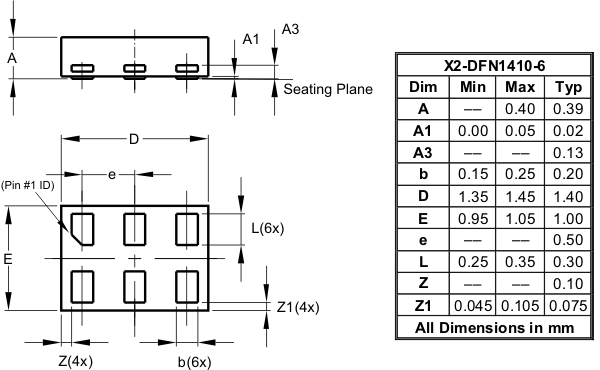
X2-DFN1410-6

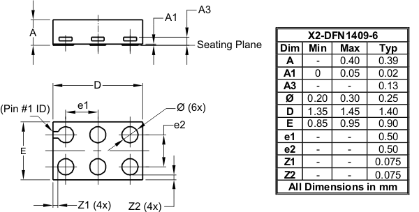
X2-DFN1409-6

X2-DFN0808-4

X1-DFN1010-6

- 74LVC1G34.pdf 74LVC1G34
- ZXSC310 led driver solution for lcd backlighting ZXSC310
- ZXSC310 led driver solution for lcd backlighting ZXSC310
- DZQA6V8AXV5 DZQA6V8AXV5
- DZQA6V8AXV5 DZQA6V8AXV5
- 74LVC2G34 dual buffer 74LVC2G34
- 74LVC2G34 dual buffer 74LVC2G34
- 74LVC2G34 dual buffer 74LVC2G34
- 74LVC2G34 dual buffer 74LVC2G34
