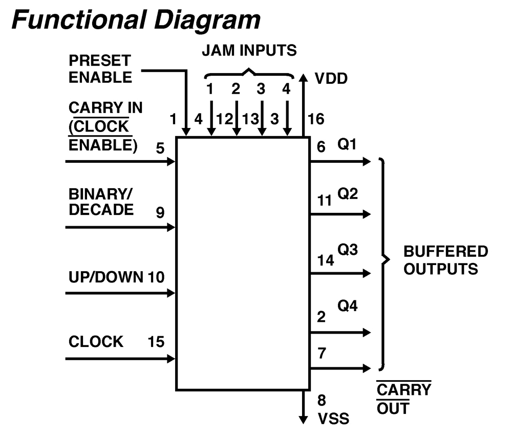
CD4029BMS consists of a four-stage binary or BCD-decade up/ down counter with provisions for look-ahead carry in both counting modes. The inputs consist of a single CLOCK, CARRY-IN (CLOCK ENABLE), BINARY/DECADE, UP/DOWN, PRESET ENABLE, and four individual JAM signals. Q1, Q2, Q3, Q4 and a CARRY-OUT OUT signal are provided as outputs.
A high PRESET ENABLE signal allows information on the JAM INPUTS to preset the counter to any state asynchronously with the clock. A low on each JAM line, when the PRESET-ENABLE signal is high, resets the counter to its zero count. The counter is advanced one count at the positive transition of the clock when the CARRY-IN-IN and PRE-SET ENABLE signals are low. Advancement is inhibited when the CARRY-IN or PRESET ENABLE signals are high. The CARRY-OUT signal is normally high and goes low when the counter reaches its maximum count in the UP mode or the minimum count in the DOWN mode provided the CARRY-IN signal is low. The CARRY-IN signal in the low state can thus be considered a CLOCK ENABLE. The CARRY-IN terminal must be connected to VSS when not in use.
Binary counting is accomplished when the BINARY/DECADE input is high; the counter counts in the decade mode when the BINARY/DECADE input is low. The counter counts up when the UP/DOWN input is high, and down when the UP/DOWN input is low. Multiple packages can be connected in either a parallelclocking or a ripple-clocking arrangement as shown in Figure 17. Parallel clocking provides synchronous control and hence faster response from all counting outputs. Ripple-clocking allows for longer clock input rise and fall times.
The CD4029BMS is supplied in these 16-lead outline packages:
Braze Seal DIP H4X
Frit Seal DIP H1F
Ceramic Flatpack H6W
Key Features
- High-Voltage Type (20V Rating)
- Medium Speed Operation: 8MHz (Typ.) at CL = 50pF and VDD - VSS = 10V
- Multi-Package Parallel Clocking for Synchronous High Speed Output Response or Ripple Clocking for Slow Clock Input Rise and Fall Times
- "Preset Enable" and Individual "Jam" Inputs Provided
- Binary or Decade Up/Down Counting
- BCD Outputs in Decade Mode
- 100% Tested for Maximum Quiescent Current at 20V
- 5V, 10V and 15V Parametric Ratings
- Standardized Symmetrical Output Characteristics
- Maximum Input Current of 1µA at 18V Over Full Package- Temperature Range; 100nA at 18V and +25oC
- Noise Margin (Over Full Package Temperature Range):
- 1V at VDD = 5V
- 2V at VDD = 10V
- 2.5V at VDD = 15V
- Meets All Requirements of JEDEC Tentative Standards No. 13B, "Standard Specifications for Description of "B" Series CMOS Device's
Applications
- Programmable Binary and Decade Counting/Frequency Synthesizers-BCD Output
- Analog to Digital and Digital to Analog Conversion
- Up/Down Binary Counting
- Difference Counting
- Magnitude and Sign Generation
- Up/Down Decade Counting

Order Information| Part Number | Package Type | Weight(g) | Pins | MSL Rating | Peak Temp (°C) | RoHS Status |
|---|
|
| CD4029BDMSR | 16 Ld SBDIP | 1.37 | 16 | N/A | NA | RoHS |
|
|
| CD4029BKMSR | 16 Ld CFP | 0.59 | 16 | N/A | NA | RoHS |
|
|
| CD4029BHNSR | Not Applicable - Contact Us | | | N/A | | RoHS |
|
|
| CD4029BHSR | Not Applicable - Contact Us | | | N/A | | RoHS |
|
|

