74LVC1T45:Voltage Translators
| Part Number | Data Sheet | SPICE Model | Number of Gates | Family | VCC Min (V) | VCC Max (V) | tpd max @ (1.5V) (ns) | tpd max @ (1.8V) (ns) | tpd max @ (2.5V) (ns) | tpd max @ (3.3V) (ns) | tpd max @ (5.0V) (ns) | Output Current |
|---|---|---|---|---|---|---|---|---|---|---|---|---|
| 74LVC1T45 | 74LVC1T45.pdf | - | 1 | LVC | 1.65 | 5.5 | - | 15.1 | 7.5 | 5.4 | 3.9 | 8 |
Description
The 74LVC1T45 is a single bit, dual supply translating transceiver with 3-state outputs suitable for transmitting a single logic bit across different voltage domains. The A input/output pin is designed to track VCCA while the B input/output tracks VCCB. This arrangement allows for universal low-voltage translation between any voltages from 1.65V to 5.5V. The Direction pin (DIR) controls the direction of the transceiver and in a logic voltage related to VCCA. When a high logic level is applied to DIR the A pin becomes an input and the B pin becomes the output. Conversely the roles of A and B are reversed when DIR is asserted low. The 3-state feature occurs when either of the power supply voltages are zero. This is also an Ioff feature and allows for the output to remain in a high impedance state with both power supplies at 0V preventing and damaging backflow currents and providing power down electrical isolation up to 5.5V as not to interfere with any logic activity on pin A or B.
Application
- Voltage Level Translation Well suited to join logic types operating at different voltages
- Power Down Signal Isolation If either voltage domain is turned off the signal is isolated and there is no loading on signal lines
- Wide array of products such as: - Cell Phones, Tablets, E-Readers - PCs, notebooks, netbooks, ultrabooks - Networking, routers, gateways - Computer peripherals, hard drives, CD/DVD ROM - TV, DVD, DVR, set top box - Personal Navigation / GPS - MP3 players ,Cameras, Video Recorders
Features
- Wide Supply Voltage Range:
- VCC(A): from 1.65V to 5.5V
- VCC(B): from 1.65V to 5.5V
- ± 24mA Output Drive at 3.3V
- CMOS low power consumption 16μA maximum ICC
- High Noise Immunity -- (100mV hysteresis typical)
- IOFF Supports Partial-Power-Down Mode Operation
- IOFF control°C by either VCC being at 0 V
- Inputs accept up to 5.5V
- ESD Protection Exceeds JESD 22
- 200-V Machine Model (A115-A)
- 2000-V Human Body Model (A114-A)
- 1000 V Charged Device Model ( C101)
- Latch-Up Exceeds 100mA per JESD 78, Class II
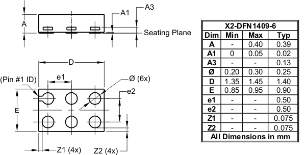
- X2-DFN1409-6 package designed as a direct replacement for chip scale packaging.
- Totally Lead-Free & Fully RoHS Compliant
- Halogen and Antimony Free. “Green” Device
Ordering Information
- 74LVC1T45FW4-7
- 74LVC1T45FX4-7
- 74LVC1T45FZ4-7
- 74LVC1T45W6-7
- 74LVC1T45Z6-7
X2-DFN1010-6

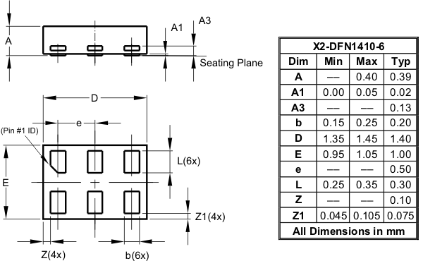
X2-DFN1410-6

X2-DFN1409-6

- 74LVC1T45.pdf 74LVC1T45
- 74LVC2G34 dual buffer 74LVC2G34
- 74LVC2G34 dual buffer 74LVC2G34
- 74LVC2G34 dual buffer 74LVC2G34
- 74LVC2G34 dual buffer 74LVC2G34
