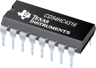
CD54HC4316 具有电平转换功能的高速 CMOS 逻辑四路模拟开关
 The ’HC4316 and CD74HCT4316 contain four independent digitally controlled analog switches that use silicon-gate CMOS technology to achieve operating speeds similar to LSTTL with the low power consumption of standard CMOS integrated circuits.
In addition these devices contain logic-level translation circuits that provide for analog signal switching of voltages between ±5V via 5V logic. Each switch is turned on by a high-level voltage on its select input (S) when the common Enable (E) is Low. A High E disables all switches. The digital inputs can swing between VCC and GND; the analog inputs/outputs can swing between VCC as a positive limit and VEE as a negative limit. Voltage ranges are shown in Figures 2 and 3
| CD54HC4316 | |
| Rating | Military |
| Technology Family | HC |
CD54HC4316 特性
- Wide Analog-Input-Voltage Range VCC – VEE...0V to 10V
- Low "ON" Resistance
- 45
 (Typ)...VCC = 4.5V
- 35
 (Typ)...VCC = 6V
- 30
 (Typ)...VCC – VEE = 9V
- 45
- Fast Switching and Propagation Delay Times
- Low "OFF" Leakage Current
- Built-In "Break-Before-Make" Switching
- Logic-Level Translation to Enable 5V Logic to Accommodate ±5V Analog Signals
- Wide Operating Temperature Range . . . –55°C to 125°C
- HC Types
- 2V to 10V Operation
- High Noise Immunity: NIL = 30%, NIH = 30% of VCC at VCC = 5V
- HCT Types
- Direct LSTTL Input Logic Compatibility, VIL = 0.8V (Max), VIH = 2V (Min)
- CMOS Input Compatibility, Il
 1µA at VOL, VOH
CD54HC4316 芯片订购指南
| 器件 | 状态 | 温度 | 价格 | 封装 | 引脚 | 封装数量 | 封装载体 | 丝印标记 |
| CD54HC4316F3A | ACTIVE | -55 to 125 | 3.75 | 1ku | CDIP (J) | 14 | 1 | TUBE |
CD54HC4316 质量与无铅数据
| 器件 | 环保计划* | 铅/焊球涂层 | MSL 等级/回流焊峰 | 环保信息与无铅 (Pb-free) | DPPM / MTBF / FIT 率 |
| CD54HC4316F3A | TBD | A42 | N/A for Pkg Type | CD54HC4316F3A | CD54HC4316F3A |
CD54HC4316 应用技术支持与电子电路设计开发资源下载
- CD54HC4316 数据资料 dataSheet 下载.PDF
- TI 德州仪器信号开关产品选型与价格 . xls
- Logic Guide 2009 (PDF 4263 KB)
- 防止模拟开关的额外功耗 (PDF 392 KB) (PDF 1305 KB)
- Understanding and Interpreting Standard-Logic Data Sheets (PDF 857 KB)
- TI IBIS File Creation, Validation, and Distribution Processes (PDF 380 KB)
- Implications of Slow or Floating CMOS Inputs (PDF 101 KB)
- CMOS Power Consumption and CPD Calculation (PDF 89 KB)
- Designing With Logic (PDF 186 KB)
- Live Insertion (PDF 150 KB)
- Input and Output Characteristics of Digital Integrated Circuits (PDF 1708 KB)
- Using High Speed CMOS and Advanced CMOS in Systems With Multiple Vcc (PDF 43 KB)
- HiRel Unitrode Power Management Brochure (PDF 206 KB)
- LOGIC Pocket Data Book (PDF 6001 KB)
- HiRel Unitrode Power Management Brochure (PDF 206 KB)
- Logic Cross-Reference (PDF 2938 KB)
