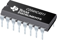
CD54HC4511 高速 CMOS 逻辑 BCD 至 7 段锁存器/解码器/驱动器

The CD54HC4511, CD74HC4511, and CD74HCT4511 are BCD-to-7 segment latch/decoder/drivers with four address inputs (D0–D3), an active-low blanking (BL)\ input, lamp-test (LT)\ input, and a latch-enable (LE)\ input that, when high, enables the latches to store the BCD inputs. When LE\ is low, the latches are disabled, making the outputs transparent to the BCD inputs.
These devices have standard-size output transistors, but are capable of sourcing (at standard VOH levels) up to 7.5 mA at 4.5 V. The HC types can supply up to 10 mA at 6 V.
|
CD54HC4511 |
| Voltage Nodes (V) |
6, 5, 2 |
| Rating |
Military |
| Technology Family |
HC |
CD54HC4511 特性
- 2-V to 6-V VCC Operation (’HC4511)
- 4.5-V to 5.5-V VCC Operation (CD74HCT4511)
- High-Output Sourcing Capability
- 7.5 mA at 4.5 V (CD74HCT4511)
- 10 mA at 6 V (’HC4511)
- Input Latches for BCD Code Storage
- Lamp Test and Blanking Capability
- Balanced Propagation Delays and Transition Times
- Significant Power Reduction Compared to LSTTL Logic ICs
- ’HC4511
- High Noise Immunity, NIL or NIH = 30% of VCC at VCC = 5 V
- CD74HCT4511
- Direct LSTTL Input Logic Compatibility, VIL = 0.8 V Maximum, VIH = 2 V Minimum
- CMOS Input Compatibility, II 1 µA at VOL, VOH
CD54HC4511 芯片订购指南
| 器件 |
状态 |
温度 (oC) |
价格(美元) |
封装 | 引脚 |
封装数量 | 封装载体 |
丝印标记 |
| 5962-8773301EA |
ACTIVE |
-55 to 125 |
10.42 | 1ku |
CDIP (J) | 16 |
1 | TUBE |
|
| CD54HC4511F3A |
ACTIVE |
-55 to 125 |
10.42 | 1ku |
CDIP (J) | 16 |
1 | TUBE |
|
CD54HC4511 应用手册
CD54HC4511 质量与无铅数据
| 器件 |
环保计划* |
铅/焊球涂层 |
MSL 等级/回流焊峰 |
环保信息与无铅 (Pb-free) |
DPPM / MTBF / FIT 率 |
| 5962-8773301EA |
TBD |
Call TI |
Call TI |
5962-8773301EA |
5962-8773301EA |
| CD54HC4511F3A |
TBD |
A42 |
N/A for Pkg Type |
CD54HC4511F3A |
CD54HC4511F3A |
CD54HC4511 应用技术支持与电子电路设计开发资源下载
- CD54HC4511数据资料 dataSheet 下载.PDF
- TI 德州仪器电源管理选型与价格参考 . xls
- (用户指南)LOGIC Pocket Data Book
- (用户指南)Signal Switch Data Book
- (选择指南)逻辑器件指南 2009 (Rev. Z)
- Logic Cross-Reference

