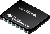
SN54ABT8996 10 位可寻址扫描端口,多点可寻址 IEEE 1149.1
 The 'ABT8996 10-bit addressable scan ports (ASP) are members of the Texas Instruments (TITM) SCOPETM testability integrated-circuit family. This family of devices supports IEEE Standard 1149.1-1990 boundary scan to facilitate testing of complex circuit assemblies. Unlike most SCOPETM devices, the ASP is not a boundary-scannable device, rather, it applies TI's addressable-shadow-port technology to the IEEE Standard 1149.1-1990 (JTAG) test access port (TAP) to extend scan access beyond the board level.
Conceptually, the ASP is a simple switch that can be used to directly connect a set of multidrop primary TAP signals to a set of secondary TAP signals - for example, to interface backplane TAP signals to a board-level TAP
|
SN54ABT8996 |
| Voltage Nodes(V) |
5 |
| Vcc range(V) |
4.5 to 5.5 |
| Input Level |
TTL |
| Output Level |
TTL |
| Rating |
Military |
| Technology Family |
JTAG |
SN54ABT8996 特性
- Members of Texas Instruments Broad Family of Testability Products Supporting IEEE Std 1149.1-1990 (JTAG) Test Access Port (TAP) and Boundary-Scan Architecture
- Extend Scan Access From Board Level to Higher Levels of System Integration
- Promote Reuse of Lower-Level (Chip/Board) Tests in System Environment
- Switch-Based Architecture Allows Direct Connect of Primary TAP to Secondary TAP
- Primary TAP Is Multidrop for Minimal Use of Backplane Wiring Channels
- Simple Addressing (Shadow) Protocol Is Received/Acknowledged on Primary TAP
- Shadow Protocols Can Occur in Any of Test-Logic-Reset, Run-Test/Idle, Pause-DR, and Pause-IR TAP States to Provide for Board-to-Board Test and Built-In Self-Test
- 10-Bit Address Space Provides for Up to 1021 User-Specified Board Addresses
- Bypass (BYP\) Pin Forces Primary-to-Secondary Connection Without Use of Shadow Protocols
- Connect (CON\) Pin Provides Indication of Primary-to-Secondary Connection
- High-Drive Outputs (-32-mA IOH, 64-mA IOL) Support Backplane Interface at Primary and High Fanout at Secondary
- Package Options Include Plastic Small- Outline (DW) and Thin Shrink Small- Outline (PW) Packages, Ceramic Chip Carriers (FK), and Ceramic DIPs (JT)
SN54ABT8996 芯片订购指南
| 器件 |
状态 |
温度 |
价格(美元) |
封装 | 引脚 |
封装数量 | 封装载体 |
丝印标记 |
| SNJ54ABT8996FK |
ACTIVE |
-55 to 125 |
27.32 | 1ku |
LCCC (FK) | 28 |
1 | TUBE |
|
| SNJ54ABT8996JT |
ACTIVE |
-55 to 125 |
20.50 | 1ku |
CDIP (JT) | 24 |
1 | TUBE |
|
| SNJ54ABT8996W |
ACTIVE |
-55 to 125 |
35.52 | 1ku |
CFP (W) | 24 |
1 | TUBE |
|
SN54ABT8996 质量与无铅数据
| 器件 |
环保计划* |
铅/焊球涂层 |
MSL 等级/回流焊峰 |
环保信息与无铅 (Pb-free) |
DPPM / MTBF / FIT 率 |
| SNJ54ABT8996FK |
TBD |
POST-PLATE |
N/A for Pkg Type |
SNJ54ABT8996FK |
SNJ54ABT8996FK |
| SNJ54ABT8996JT |
TBD |
A42 |
N/A for Pkg Type |
SNJ54ABT8996JT |
SNJ54ABT8996JT |
| SNJ54ABT8996W |
TBD |
A42 |
N/A for Pkg Type |
SNJ54ABT8996W |
SNJ54ABT8996W |
SN54ABT8996 应用技术支持与电子电路设计开发资源下载
- SN54ABT8996 数据资料 dataSheet 下载.PDF
- TI 德州仪器特殊逻辑产品选型与价格 . xls
- Shelf-Life Evaluation of Lead-Free Component Finishes (PDF 1305 KB)
- Understanding and Interpreting Standard-Logic Data Sheets (PDF 857 KB)
- TI IBIS File Creation, Validation, and Distribution Processes (PDF 380 KB)
- Implications of Slow or Floating CMOS Inputs (PDF 101 KB)
- CMOS Power Consumption and CPD Calculation (PDF 89 KB)
- Designing With Logic (PDF 186 KB)
- Live Insertion (PDF 150 KB)
- Input and Output Characteristics of Digital Integrated Circuits (PDF 1708 KB)
- Using High Speed CMOS and Advanced CMOS in Systems With Multiple Vcc (PDF 43 KB)
- HiRel Unitrode Power Management Brochure (PDF 206 KB)
- LOGIC Pocket Data Book (PDF 6001 KB)
- HiRel Unitrode Power Management Brochure (PDF 206 KB)
- Logic Cross-Reference (PDF 2938 KB)
 The 'ABT8996 10-bit addressable scan ports (ASP) are members of the Texas Instruments (TITM) SCOPETM testability integrated-circuit family. This family of devices supports IEEE Standard 1149.1-1990 boundary scan to facilitate testing of complex circuit assemblies. Unlike most SCOPETM devices, the ASP is not a boundary-scannable device, rather, it applies TI's addressable-shadow-port technology to the IEEE Standard 1149.1-1990 (JTAG) test access port (TAP) to extend scan access beyond the board level.