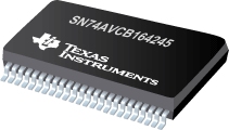
SN74AVCB164245 16 位双电源总线收发器,具有可配置 转换和三态输出
 This 16-bit (dual-octal) noninverting bus transceiver uses two separate configurable power-supply rails. The A port is designed to track VCCA. VCCA accepts any supply voltage from 1.4 V to 3.6 V. The B port is designed to track VCCB. VCCB accepts any supply voltage from 1.4 V to 3.6 V. This allows for universal low-voltage bidirectional translation between any of the 1.5-V, 1.8-V, 2.5-V, and 3.3-V voltage nodes.
The SN74AVCB164245 is designed for asynchronous communication between data buses. The device transmits data from the A bus to the B bus or from the B bus to the A bus, depending on the logic level at the direction-control (DIR) input. The output-enable (OE) input can be used to disable the outputs so the buses are effectively isolated
|
SN74AVCB164245 |
| Voltage Nodes(V) |
3.3, 2.5, 1.8, 1.5 |
| Vcc range(V) |
1.4 to 3.6 |
| Logic |
True |
| No. of Bits |
16 |
| No. of Outputs |
16 |
| Bus Drive(ma) |
-12/12 |
| Static Current |
+0.04 |
| tpd max(ns) |
7.6 |
| Technology Family |
AVC |
| Pin/Package |
48TSSOP, 48TVSOP |
| Operating Temperature Range(°C) |
-40 to 85 |
| Approx. Price (US$) |
3.10 | 1ku |
| Rating |
Catalog |
SN74AVCB164245 特性
- Member of the Texas Instruments Widebus™ Family
- DOC™ Circuitry Dynamically Changes Output Impedance, Resulting in Noise Reduction Without Speed Degradation
- Dynamic Drive Capability Is Equivalent to Standard Outputs With IOH and IOL of ±24 mA at 2.5-V VCC
- Control Inputs VIH/VIL Levels Are Referenced to VCCB Voltage
- If Either VCC Input Is at GND, Both Ports Are in the High-Impedance State
- Overvoltage-Tolerant Inputs/Outputs Allow Mixed-Voltage-Mode Data Communications
- Ioff Supports Partial-Power-Down Mode Operation
- Fully Configurable Dual-Rail Design Allows Each Port to Operate Over Full 1.4-V to 3.6-V Power-Supply Range
- Latch-Up Performance Exceeds 100 mA Per JESD 78, Class II
- ESD Protection Exceeds JESD 22
- 2000-V Human-Body Model (A114-A)
- 200-V Machine Model (A115-A)
- 1000-V Charged-Device Model (C101)
SN74AVCB164245 芯片订购指南
| 器件 |
状态 |
温度 |
价格(美元) |
封装 | 引脚 |
封装数量 | 封装载体 |
丝印标记 |
| 74AVCB164245GRE4 |
ACTIVE |
-40 to 85 |
1.50 | 1ku |
TSSOP (PW) | 48 |
2000 | LARGE T&R |
|
| 74AVCB164245GRG4 |
ACTIVE |
-40 to 85 |
1.50 | 1ku |
TSSOP (PW) | 48 |
2000 | LARGE T&R |
|
| 74AVCB164245VRE4 |
ACTIVE |
-40 to 85 |
1.50 | 1ku |
TVSOP (DGV) | 48 |
2000 | LARGE T&R |
|
| 74AVCB164245VRG4 |
ACTIVE |
-40 to 85 |
1.50 | 1ku |
TVSOP (DGV) | 48 |
2000 | LARGE T&R |
|
SN74AVCB164245 质量与无铅数据
| 器件 |
环保计划* |
铅/焊球涂层 |
MSL 等级/回流焊峰 |
环保信息与无铅 (Pb-free) |
DPPM / MTBF / FIT 率 |
| 74AVCB164245GRE4 |
Green (RoHS & no Sb/Br) |
CU NIPDAU |
Level-1-260C-UNLIM |
74AVCB164245GRE4 |
74AVCB164245GRE4 |
| 74AVCB164245GRG4 |
Green (RoHS & no Sb/Br) |
CU NIPDAU |
Level-1-260C-UNLIM |
74AVCB164245GRG4 |
74AVCB164245GRG4 |
| 74AVCB164245VRE4 |
Green (RoHS & no Sb/Br) |
CU NIPDAU |
Level-1-260C-UNLIM |
74AVCB164245VRE4 |
74AVCB164245VRE4 |
| 74AVCB164245VRG4 |
Green (RoHS & no Sb/Br) |
CU NIPDAU |
Level-1-260C-UNLIM |
74AVCB164245VRG4 |
74AVCB164245VRG4 |
SN74AVCB164245 应用技术支持与电子电路设计开发资源下载
- SN74AVCB164245 数据资料 dataSheet 下载.PDF
- TI 德州仪器电压电平转换产品选型与价格 . xls
- Shelf-Life Evaluation of Lead-Free Component Finishes (PDF 1305 KB)
- Understanding and Interpreting Standard-Logic Data Sheets (PDF 857 KB)
- TI IBIS File Creation, Validation, and Distribution Processes (PDF 380 KB)
- Implications of Slow or Floating CMOS Inputs (PDF 101 KB)
- CMOS Power Consumption and CPD Calculation (PDF 89 KB)
- Designing With Logic (PDF 186 KB)
- Live Insertion (PDF 150 KB)
- Input and Output Characteristics of Digital Integrated Circuits (PDF 1708 KB)
- Using High Speed CMOS and Advanced CMOS in Systems With Multiple Vcc (PDF 43 KB)
- HiRel Unitrode Power Management Brochure (PDF 206 KB)
- LOGIC Pocket Data Book (PDF 6001 KB)
- HiRel Unitrode Power Management Brochure (PDF 206 KB)
- Logic Cross-Reference (PDF 2938 KB)
 This 16-bit (dual-octal) noninverting bus transceiver uses two separate configurable power-supply rails. The A port is designed to track VCCA. VCCA accepts any supply voltage from 1.4 V to 3.6 V. The B port is designed to track VCCB. VCCB accepts any supply voltage from 1.4 V to 3.6 V. This allows for universal low-voltage bidirectional translation between any of the 1.5-V, 1.8-V, 2.5-V, and 3.3-V voltage nodes.
