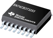
SN74CB3T3253 双路 4 选 1 FET 多路复用器/多路解复用器,具有 5V 容限电平转换器的 2.5V/3.3V 低电压总线开关
 The SN74CB3T3253 is a high-speed TTL-compatible FET multiplexer/demultiplexer with low ON-state resistance (ron), allowing for minimal propagation delay. The device fully supports mixed-mode signal operation on all data I/O ports by providing voltage translation that tracks VCC. The SN74CB3T3253 supports systems using 5-V TTL, 3.3-V LVTTL, and 2.5-V CMOS switching standards, as well as user-defined switching levels (see Figure 1).
The SN74CB3T3253 is organized as two 1-of-4 multiplexer/demultiplexers with separate output-enable (1OE\, 2OE\) inputs. The select (S0, S1) inputs control the data path of each multiplexer/demultiplexer. When OE\ is low, the associated multiplexer/demultiplexer is ON, and the A port is connected to the B port, allowing bidirectional data flow between ports
|
SN74CB3T3253 |
| ron(max)(ohms) |
8 |
| tpd max(ns) |
0.25 |
| Pin/Package |
16SOIC |
| Technology Family |
CB3T |
| Operating Temperature Range(°C) |
-40 to 85 |
| Approx. Price (US$) |
1.10 | 1ku |
SN74CB3T3253 特性
- Output Voltage Translation Tracks VCC
- Supports Mixed-Mode Signal Operation On All Data I/O Ports
- 5-V Input Down To 3.3-V Output Level Shift With 3.3-V VCC
- 5-V/3.3-V Input Down To 2.5-V Output Level Shift With 2.5-V VCC
- 5-V Tolerant I/Os With Device Powered-Up or Powered-Down
- Bidirectional Data Flow, With Near-Zero Propagation Delay
- Low ON-State Resistance (ron) Characteristics (ron = 5 Typical)
- Low Input/Output Capacitance Minimizes Loading (Cio(OFF) = 5 pF Typical)
- Data and Control Inputs Provide Undershoot Clamp Diodes
- Low Power Consumption (ICC = 20 µA Max)
- VCC Operating Range From 2.3 V to 3.6 V
- Data I/Os Support 0 to 5-V Signaling Levels (0.8-V, 1.2-V, 1.5-V, 1.8-V, 2.5-V, 3.3-V, 5-V)
- Control Inputs Can be Driven by TTL or 5-V/3.3-V CMOS Outputs
- Ioff Supports Partial-Power-Down Mode Operation
- Latch-Up Performance Exceeds 250 mA Per JESD 17
- ESD Performance Tested Per JESD 22
- 2000-V Human-Body Model (A114-B, Class II)
- 1000-V Charged-Device Model (C101)
- Supports Digital Applications: Level Translation, USB Interface, Memory Interleaving, Bus Isolation
- Ideal for Low-Power Portable Equipment
SN74CB3T3253 芯片订购指南
SN74CB3T3253 质量与无铅数据
| 器件 |
环保计划* |
铅/焊球涂层 |
MSL 等级/回流焊峰 |
环保信息与无铅 (Pb-free) |
DPPM / MTBF / FIT 率 |
| SN74CB3T3253D |
Green (RoHS & no Sb/Br) |
CU NIPDAU |
Level-1-260C-UNLIM |
SN74CB3T3253D |
SN74CB3T3253D |
| SN74CB3T3253DE4 |
Green (RoHS & no Sb/Br) |
CU NIPDAU |
Level-1-260C-UNLIM |
SN74CB3T3253DE4 |
SN74CB3T3253DE4 |
| SN74CB3T3253DG4 |
Green (RoHS & no Sb/Br) |
CU NIPDAU |
Level-1-260C-UNLIM |
SN74CB3T3253DG4 |
SN74CB3T3253DG4 |
| SN74CB3T3253DR |
Green (RoHS & no Sb/Br) |
CU NIPDAU |
Level-1-260C-UNLIM |
SN74CB3T3253DR |
SN74CB3T3253DR |
| SN74CB3T3253DRE4 |
Green (RoHS & no Sb/Br) |
CU NIPDAU |
Level-1-260C-UNLIM |
SN74CB3T3253DRE4 |
SN74CB3T3253DRE4 |
| SN74CB3T3253DRG4 |
Green (RoHS & no Sb/Br) |
CU NIPDAU |
Level-1-260C-UNLIM |
SN74CB3T3253DRG4 |
SN74CB3T3253DRG4 |
SN74CB3T3253 应用技术支持与电子电路设计开发资源下载
- SN74CB3T3253 数据资料 dataSheet 下载.PDF
- TI 德州仪器信号开关产品选型与价格 . xls
- Logic Guide 2009 (PDF 4263 KB)
- 防止模拟开关的额外功耗 (PDF 392 KB) (PDF 1305 KB)
- Understanding and Interpreting Standard-Logic Data Sheets (PDF 857 KB)
- TI IBIS File Creation, Validation, and Distribution Processes (PDF 380 KB)
- Implications of Slow or Floating CMOS Inputs (PDF 101 KB)
- CMOS Power Consumption and CPD Calculation (PDF 89 KB)
- Designing With Logic (PDF 186 KB)
- Live Insertion (PDF 150 KB)
- Input and Output Characteristics of Digital Integrated Circuits (PDF 1708 KB)
- Using High Speed CMOS and Advanced CMOS in Systems With Multiple Vcc (PDF 43 KB)
- HiRel Unitrode Power Management Brochure (PDF 206 KB)
- LOGIC Pocket Data Book (PDF 6001 KB)
- HiRel Unitrode Power Management Brochure (PDF 206 KB)
- Logic Cross-Reference (PDF 2938 KB)
 The SN74CB3T3253 is a high-speed TTL-compatible FET multiplexer/demultiplexer with low ON-state resistance (ron), allowing for minimal propagation delay. The device fully supports mixed-mode signal operation on all data I/O ports by providing voltage translation that tracks VCC. The SN74CB3T3253 supports systems using 5-V TTL, 3.3-V LVTTL, and 2.5-V CMOS switching standards, as well as user-defined switching levels (see Figure 1).