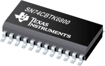
SN74CBTK6800 具有预充电输出和有源钳位下冲电路的 10 位 FET 总线开关
 The SN74CBTK6800 device provides ten bits of high-speed TTL-compatible bus switching. The low on-state resistance of the switch allows bidirectional connections to be made while adding near-zero propagation delay. The device also precharges the B port to a user-selectable bias voltage (BIASV) to minimize live-insertion noise.
The A and B ports have an active-clamp undershoot-protection circuit. When there is an undershoot, the active-clamp circuit is enabled and current from VCC is supplied to clamp the output, preventing the pass transistor from turning on.
The SN74CBTK6800 is organized as one 10-bit switch with a single enable (ON\) input. When ON\ is low, the switch is on, and port A is connected to port B. When ON\ is high, the switch between port A and port B is open
| SN74CBTK6800 | |
| Voltage Nodes(V) | 5 |
| Vcc range(V) | 4.0 to 5.5 |
| No. of Bits | 10 |
| Input Level | TTL |
| Output Level | TTL |
| ron(max)(ohms) | 20 |
| Static Current(Max) | 0.02 |
| tpd max(ns) | 0.25 |
| Rating | Catalog |
| Technology Family | CBT |
SN74CBTK6800 特性
- 5-
 Switch Connection Between Two Ports
- TTL-Compatible Input Levels
- Power Off Disables Outputs, Permitting Live Insertion
- Outputs Are Precharged by Bias Voltage to Minimize Signal Distortion During Live Insertion
- Active-Clamp Undershoot-Protection Circuit on the I/Os Clamps Undershoots Down to \x962 V
- Latch-Up Performance Exceeds 100 mA Per JESD 78, Class II
- ESD Protection Exceeds JESD 22
- 2000-V Human-Body Model (A114-A)
- 200-V Machine Model (A115-A)
- 1000-V Charged-Device Model (C101)
SN74CBTK6800 芯片订购指南
| 器件 | 状态 | 温度 | 价格 | 封装 | 引脚 | 封装数量 | 封装载体 | 丝印标记 |
| SN74CBTK6800DWR | ACTIVE | -40 to 85 | 1.45 | 1ku | SOIC (DW) | 24 | 2000 | LARGE T&R | |
| SN74CBTK6800DWRE4 | ACTIVE | -40 to 85 | 1.45 | 1ku | SOIC (DW) | 24 | 2000 | LARGE T&R | |
| SN74CBTK6800DWRG4 | ACTIVE | -40 to 85 | 1.45 | 1ku | SOIC (DW) | 24 | 2000 | LARGE T&R |
SN74CBTK6800 质量与无铅数据
| 器件 | 环保计划* | 铅/焊球涂层 | MSL 等级/回流焊峰 | 环保信息与无铅 (Pb-free) | DPPM / MTBF / FIT 率 |
| SN74CBTK6800DWR | Green (RoHS & no Sb/Br) | CU NIPDAU | Level-1-260C-UNLIM | SN74CBTK6800DWR | SN74CBTK6800DWR |
| SN74CBTK6800DWRE4 | Green (RoHS & no Sb/Br) | CU NIPDAU | Level-1-260C-UNLIM | SN74CBTK6800DWRE4 | SN74CBTK6800DWRE4 |
| SN74CBTK6800DWRG4 | Green (RoHS & no Sb/Br) | CU NIPDAU | Level-1-260C-UNLIM | SN74CBTK6800DWRG4 | SN74CBTK6800DWRG4 |
SN74CBTK6800 应用技术支持与电子电路设计开发资源下载
- SN74CBTK6800 数据资料 dataSheet 下载.PDF
- TI 德州仪器信号开关产品选型与价格 . xls
- Logic Guide 2009 (PDF 4263 KB)
- 防止模拟开关的额外功耗 (PDF 392 KB) (PDF 1305 KB)
- Understanding and Interpreting Standard-Logic Data Sheets (PDF 857 KB)
- TI IBIS File Creation, Validation, and Distribution Processes (PDF 380 KB)
- Implications of Slow or Floating CMOS Inputs (PDF 101 KB)
- CMOS Power Consumption and CPD Calculation (PDF 89 KB)
- Designing With Logic (PDF 186 KB)
- Live Insertion (PDF 150 KB)
- Input and Output Characteristics of Digital Integrated Circuits (PDF 1708 KB)
- Using High Speed CMOS and Advanced CMOS in Systems With Multiple Vcc (PDF 43 KB)
- HiRel Unitrode Power Management Brochure (PDF 206 KB)
- LOGIC Pocket Data Book (PDF 6001 KB)
- HiRel Unitrode Power Management Brochure (PDF 206 KB)
- Logic Cross-Reference (PDF 2938 KB)
