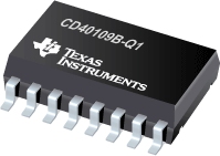
CD40109B-Q1 CMOS 四路低向高电压位转换器(20V 额定电压)
 CD40109B contains four low-to-high-voltage level-shifting circuits. Each circuit will shift a low-voltage digital-logic input signal (A, B, C, D) with logical 1 = VCC and logical 0 = VSS to a high-voltage output signal (E, F, G, H) with logical 1 = VDD and logical 0 = VSS.
The RCA-CD40109, unlike other low-to-high level-shifting circuits, does not require the presence of the high-voltage supply (VDD) before the application of either the low-voltage supply (VCC) or the input signals. There are no restrictions on the sequence of application of VDD, VCC, or the input signals. In addition, with one exception there are no restrictions on the relative magnitudes of the supply voltages or input signals within the device maximum ratings, provided that the input signal swings between VSS and at least 0
|
CD40109B-Q1 |
| Voltage Nodes(V) |
5,10,15 |
| Technology Family |
CD4000 |
| Pin/Package |
16SO |
| Operating Temperature Range(°C) |
-40 to 125 |
| Approx. Price (US$) |
0.34 | 1ku |
| Rating |
Automotive |
CD40109B-Q1 特性
- Qualified for Automotive Applications
- Independent of Power Supply Sequence Considerations
- VCC Can Exceed VDD
- Input Signals can Exceed Both VCC and VDD
- Up and Down Level-Shifting Capability
- Three-State Outputs With Separate Enable Controls
- Standardized Symmetrical Output Characteristics
- 100% Tested for Quiescent Current at 20 V
- Maximum Input Current:
- 1 µA at 18 V Over Full Package-Temperature Range
- 100 nA at 18 V and 25°C
- Noise Margin (Full Package-Temperature Range):
- 1 V at VCC = 5 V, VDD = 10 V
- 2 V at VCC = 10 V, VDD = 15 V
- 5-V, 10-V, and 15-V Parametric Ratings
- Meets All Requirements of JEDEC Tentative Standard No. 13B, "Standard specifications for Description of ‘B’ Series CMOS Devices"
- Latch-Up Performance Meets 50 mA per JESD 78, Class I
- APPLICATIONS
- High-or-Low Level-Shifting With Three-State Outputs for
Unidirectional or Bidirectional Bussing
- Isolation of Logic Subsystem Using Separate Power Supplies from
Supply Sequencing, Supply Loss, and Supply Regulation Considerations
CD40109B-Q1 芯片订购指南
| 器件 |
状态 |
温度 |
价格(美元) |
封装 | 引脚 |
封装数量 | 封装载体 |
丝印标记 |
| CD40109BQNSRQ1 |
ACTIVE |
-40 to 125 |
0.34 | 1ku |
SO (NS) | 16 |
2000 | LARGE T&R |
|
CD40109B-Q1 质量与无铅数据
| 器件 |
环保计划* |
铅/焊球涂层 |
MSL 等级/回流焊峰 |
环保信息与无铅 (Pb-free) |
DPPM / MTBF / FIT 率 |
| CD40109BQNSRQ1 |
Green (RoHS & no Sb/Br) |
CU NIPDAU |
Level-1-260C-UNLIM |
CD40109BQNSRQ1 |
CD40109BQNSRQ1 |
CD40109B-Q1 应用技术支持与电子电路设计开发资源下载
- CD40109B-Q1 数据资料 dataSheet 下载.PDF
- TI 德州仪器电压电平转换产品选型与价格 . xls
- Shelf-Life Evaluation of Lead-Free Component Finishes (PDF 1305 KB)
- Understanding and Interpreting Standard-Logic Data Sheets (PDF 857 KB)
- TI IBIS File Creation, Validation, and Distribution Processes (PDF 380 KB)
- Implications of Slow or Floating CMOS Inputs (PDF 101 KB)
- CMOS Power Consumption and CPD Calculation (PDF 89 KB)
- Designing With Logic (PDF 186 KB)
- Live Insertion (PDF 150 KB)
- Input and Output Characteristics of Digital Integrated Circuits (PDF 1708 KB)
- Using High Speed CMOS and Advanced CMOS in Systems With Multiple Vcc (PDF 43 KB)
- HiRel Unitrode Power Management Brochure (PDF 206 KB)
- LOGIC Pocket Data Book (PDF 6001 KB)
- HiRel Unitrode Power Management Brochure (PDF 206 KB)
- Logic Cross-Reference (PDF 2938 KB)
 CD40109B contains four low-to-high-voltage level-shifting circuits. Each circuit will shift a low-voltage digital-logic input signal (A, B, C, D) with logical 1 = VCC and logical 0 = VSS to a high-voltage output signal (E, F, G, H) with logical 1 = VDD and logical 0 = VSS.
