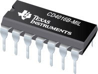
CD4016B-MIL CMOS 四路双向开关
 CD4016B Series types are quad bilateral switches intended for the transmission or multiplexing of analog or digital signals. Each of the four independent bilateral switches has a single control signal input which simultaneously biases both the p and n device in a given switch on or off.
The CD4016 "B" Series types are supplied in 14-lead hermetic dual-in-line ceramic packages (F3A suffix), 14-lead dual-in-line plastic packages (E suffix), 14-lead small-outline packages (M, MT, M96, and NSR suffixes), and 14-lead thin shrink small-outline packages (PW and PWR suffixes).
|
CD4016B-MIL |
| Voltage Nodes(V) |
5, 10, 15 |
| Vcc range(V) |
3.0 to 18.0 |
| Configuration |
4 X SPST (NO) |
| No. of Bits |
4 |
| Input Level |
CMOS |
| Output Level |
CMOS |
| ron(max)(ohms) |
400 |
| RON Mis-match(Max)(Ohms) |
5 |
| ON Time(Max)(ns) |
30 |
| OFF Time(Max)(ns) |
30 |
| IL OFF(Max)(nA) |
+/-1000 |
| Rating |
Catalog |
| Technology Family |
CD4000 |
CD4016B-MIL 特性
- 20-V digital or ± 10-V peak-to-peak switching
- 280-
 typical on-state resistance for 15-V operation
- Switch on-state resistance matched to within 10
 typ. over 15-V signal-input range
- High on/off output-voltage ratio:
65 dB typ. @ fis = 10 kHz, RL = 10 k

- High degree of linearity:
<0.5% distortion typ. @ fis = 1 kHz, Vis = 5 Vp-p, VDD–VSS

- Extremely low off-state switch leakage resulting in very low offset current and high effective off-state resistance:
100pA typ. @ VDD–VSS = 18 V, TA = 25°C
- Extremely high control input impedance (control circuit isolated form signal circuit:
1012
 typ.
typ.
- Low crosstalk between switches:
–50 dB typ. @ fis= 0.9 MHz, RL = 1 k

- Matched control-input to signal-output capacitance:
Reduces output signal transients
- Frequency response, switch on = 40MHz (typ.)
- 100% tested for quiescent current at 20 V
- Maximum control input current of 1 µA at 18 V over full package temperature range; 100 nA at 18 V and 25°C
- 5-V, 10-V, and 15-V parametric ratings
- Applications:
- Analog signal switching/multiplexing
- Signal gating
- Squelch control
- Chopper
- Modulator
- Demodulator
CD4016B-MIL 芯片订购指南
| 器件 |
状态 |
温度 |
价格 |
封装 | 引脚 |
封装数量 | 封装载体 |
丝印标记 |
| 5962-9064001CA |
ACTIVE |
-55 to 125 |
4.73 | 1ku |
CDIP (J) | 14 |
1 | TUBE |
|
| CD4016BF |
ACTIVE |
-55 to 125 |
4.03 | 1ku |
CDIP (J) | 14 |
1 | TUBE |
|
| CD4016BF3A |
ACTIVE |
-55 to 125 |
4.73 | 1ku |
CDIP (J) | 14 |
1 | TUBE |
|
CD4016B-MIL 质量与无铅数据
| 器件 |
环保计划* |
铅/焊球涂层 |
MSL 等级/回流焊峰 |
环保信息与无铅 (Pb-free) |
DPPM / MTBF / FIT 率 |
| 5962-9064001CA |
TBD |
A42 |
N/A for Pkg Type |
5962-9064001CA |
5962-9064001CA |
| CD4016BF |
TBD |
A42 |
N/A for Pkg Type |
CD4016BF |
CD4016BF |
| CD4016BF3A |
TBD |
A42 |
N/A for Pkg Type |
CD4016BF3A |
CD4016BF3A |
CD4016B-MIL 应用技术支持与电子电路设计开发资源下载
- CD4016B-MIL 数据资料 dataSheet 下载.PDF
- TI 德州仪器信号开关产品选型与价格 . xls
- Logic Guide 2009 (PDF 4263 KB)
- 防止模拟开关的额外功耗 (PDF 392 KB) (PDF 1305 KB)
- Understanding and Interpreting Standard-Logic Data Sheets (PDF 857 KB)
- TI IBIS File Creation, Validation, and Distribution Processes (PDF 380 KB)
- Implications of Slow or Floating CMOS Inputs (PDF 101 KB)
- CMOS Power Consumption and CPD Calculation (PDF 89 KB)
- Designing With Logic (PDF 186 KB)
- Live Insertion (PDF 150 KB)
- Input and Output Characteristics of Digital Integrated Circuits (PDF 1708 KB)
- Using High Speed CMOS and Advanced CMOS in Systems With Multiple Vcc (PDF 43 KB)
- HiRel Unitrode Power Management Brochure (PDF 206 KB)
- LOGIC Pocket Data Book (PDF 6001 KB)
- HiRel Unitrode Power Management Brochure (PDF 206 KB)
- Logic Cross-Reference (PDF 2938 KB)
 CD4016B Series types are quad bilateral switches intended for the transmission or multiplexing of analog or digital signals. Each of the four independent bilateral switches has a single control signal input which simultaneously biases both the p and n device in a given switch on or off.
 typical on-state resistance for 15-V operation
 typ. over 15-V signal-input range


 typ.
typ.

