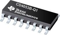
CD4053B-Q1 具有逻辑电平转换的汽车类 CMOS 单路 8 通道模拟多路复用器/多路解复用器
 The CD4051B, CD4052B, and CD4053B analog multiplexers are digitally-controlled analog switches that have low ON impedance and very low OFF leakage current. Control of analog signals up to 20 VP-P can be achieved by digital signal amplitudes of 4.5 V to 20 V (If VDD - VSS = 3 V, a VDD - VEE of up to 13 V can be controlled; for VDD - VEE level differences above 13 V, a VDD - VSS of at least 4.5 V is required). For example, if VDD = 4.5 V, VSS = 0 V, and VEE = –13.5 V, analog signals from –13.5 V to 4.5 V can be controlled by digital inputs of 0 V to 5 V. These multiplexer circuits dissipate extremely low quiescent power over the full VDD - VSS and VDD - VEE supply-voltage ranges, independent of the logic state of the control signals.
|
CD4053B-Q1 |
| Number of Channels |
8 |
| Configuration |
1 X 1:8 MUX |
| ron(max)(ohms) |
240 |
| ICC(uA) |
100 |
| tpd max(ns) |
20 |
| Technology Family |
CD4000 |
| Voltage Nodes(V) |
5, 10, 15 |
| RON Mis-match(Max)(Ohms) |
5 |
| ON Time(Max)(ns) |
240 |
| OFF Time(Max)(ns) |
160 |
| Rating |
Automotive |
| VCC(Min)(V) |
5 |
| VCC(Max)(V) |
20 |
| Pin/Package |
16TSSOP |
| Approx. Price (US$) |
0.31 | 1ku |
| Operating Temperature Range(°C) |
-40 to 125 |
CD4053B-Q1 特性
- Qualified for Automotive Applications
- Wide Range of Digital and Analog Signal Levels
- Digital: 3 V to 20 V
- Analog: ≤ 20 VP-P
- Low ON Resistance, 125
 (Typ) Over 15 VP-P Signal Input Range for VDD - VEE = 18 V
- High OFF Resistance, Channel Leakage of ±100 pA (Typ) at VDD - VEE = 18 V
- Logic-Level Conversion for Digital Addressing Signals of 3 V to 20 V (VDD - VSS = 3 V to 20 V) to Switch Analog Signals to 20 VP-P (VDD - VEE = 20 V)
- Matched Switching Characteristics, ron = 5
 (Typ) for VDD - VEE = 15 V
- Very Low Quiescent Power Dissipation Under All Digital-Control Input and Supply Conditions, 0.2 µW (Typ) at VDD - VSS = VDD - VEE = 10 V
- Binary Address Decoding on Chip
- 5-V, 10-V, and 15-V Parametric Ratings
- 100% Tested for Quiescent Current at 20 V
- Maximum Input Current of 1µA at 18 V Over Full Package Temperature Range, 100 nA at 18 V and 25°C
- Break-Before-Make Switching Eliminates Channel Overlap
- Applications
- Analog and Digital Multiplexing and Demultiplexing
- Analog-to-Digital (A/D) and Digital-to-Analog (D/A) Conversion
- Signal Gating
CD4053B-Q1 芯片订购指南
| 器件 |
状态 |
温度 |
价格 |
封装 | 引脚 |
封装数量 | 封装载体 |
丝印标记 |
| CD4053BQM96G4Q1 |
ACTIVE |
-40 to 125 |
0.31 | 1ku |
TSSOP (PW) | 16 |
2000 |
|
| CD4053BQM96Q1 |
ACTIVE |
-40 to 125 |
0.31 | 1ku |
TSSOP (PW) | 16 |
2000 |
|
CD4053B-Q1 质量与无铅数据
| 器件 |
环保计划* |
铅/焊球涂层 |
MSL 等级/回流焊峰 |
环保信息与无铅 (Pb-free) |
DPPM / MTBF / FIT 率 |
| CD4053BQM96G4Q1 |
Green (RoHS & no Sb/Br) |
CU NIPDAU |
Level-1-260C-UNLIM |
CD4053BQM96G4Q1 |
CD4053BQM96G4Q1 |
| CD4053BQM96Q1 |
Pb-Free (RoHS) |
CU NIPDAU |
Level-1-250C-UNLIM |
CD4053BQM96Q1 |
CD4053BQM96Q1 |
CD4053B-Q1 应用技术支持与电子电路设计开发资源下载
- CD4053B-Q1 数据资料 dataSheet 下载.PDF
- TI 德州仪器信号开关产品选型与价格 . xls
- Logic Guide 2009 (PDF 4263 KB)
- 防止模拟开关的额外功耗 (PDF 392 KB) (PDF 1305 KB)
- Understanding and Interpreting Standard-Logic Data Sheets (PDF 857 KB)
- TI IBIS File Creation, Validation, and Distribution Processes (PDF 380 KB)
- Implications of Slow or Floating CMOS Inputs (PDF 101 KB)
- CMOS Power Consumption and CPD Calculation (PDF 89 KB)
- Designing With Logic (PDF 186 KB)
- Live Insertion (PDF 150 KB)
- Input and Output Characteristics of Digital Integrated Circuits (PDF 1708 KB)
- Using High Speed CMOS and Advanced CMOS in Systems With Multiple Vcc (PDF 43 KB)
- HiRel Unitrode Power Management Brochure (PDF 206 KB)
- LOGIC Pocket Data Book (PDF 6001 KB)
- HiRel Unitrode Power Management Brochure (PDF 206 KB)
- Logic Cross-Reference (PDF 2938 KB)
 The CD4051B, CD4052B, and CD4053B analog multiplexers are digitally-controlled analog switches that have low ON impedance and very low OFF leakage current. Control of analog signals up to 20 VP-P can be achieved by digital signal amplitudes of 4.5 V to 20 V (If VDD - VSS = 3 V, a VDD - VEE of up to 13 V can be controlled; for VDD - VEE level differences above 13 V, a VDD - VSS of at least 4.5 V is required). For example, if VDD = 4.5 V, VSS = 0 V, and VEE = –13.5 V, analog signals from –13.5 V to 4.5 V can be controlled by digital inputs of 0 V to 5 V. These multiplexer circuits dissipate extremely low quiescent power over the full VDD - VSS and VDD - VEE supply-voltage ranges, independent of the logic state of the control signals.
 (Typ) Over 15 VP-P Signal Input Range for VDD - VEE = 18 V
 (Typ) for VDD - VEE = 15 V
