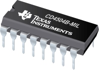
CD4504B-MIL CMOS 四路低向高电压位转换器(20V 额定电压)
 CD4504B hex voltage level-shifter consists of six circuits which shift input signals from the VCC logic level to the VDD logic level. To shift TTL signals to CMOS logic levels, the SELECT input is at the VCC HIGH logic state. When the SELECT input is a LOW logic state, each circuit translates signals from one CMOS level to another.
The CD4504B types are supplied in 16-lead hermetic dual-in-line ceramic packages (F3A suffix), 16-lead dual-in-line plastic packages (E suffix), 16-lead small-outline packages (M, M96, and MT suffixes), and 16-lead thin shrink small-outline packages (PW and PWR suffixes).
|
CD4504B-MIL |
| Input Level |
5,10,15 |
| No. of Outputs |
CD4000 |
| Pin/Package |
16CDIP |
| Operating Temperature Range(°C) |
-55 to 125 |
| Rating |
Military |
CD4504B-MIL 特性
- Independence of power-supply sequence considerations - VCC can exceed VDD; input signals can exceed both VCC and VDD
- Up and down level-shifting capability
- Shiftable input threshold for either CMOS or TTL compatibility
- Standardized symmetrical output characteristics
- 100% tested for quiescent current @ 20 V
- Maximum input current of 1 µA at 18 V over full package-temperature range; 100 nA at 18 V and 25°C
- 5V, 10 V, and 15 V parametric ratings
- Meets all requirements of JEDEC Standard No. 13B, "Standard Specifications for Description of ’B’ Series CMOS Devices
CD4504B-MIL 芯片订购指南
| 器件 |
状态 |
温度 |
价格(美元) |
封装 | 引脚 |
封装数量 | 封装载体 |
丝印标记 |
| CD4504BF3A |
ACTIVE |
-55 to 125 |
5.19 | 100u |
CDIP (J) | 16 |
1 | TUBE |
|
CD4504B-MIL 质量与无铅数据
| 器件 |
环保计划* |
铅/焊球涂层 |
MSL 等级/回流焊峰 |
环保信息与无铅 (Pb-free) |
DPPM / MTBF / FIT 率 |
| CD4504BF3A |
TBD |
A42 |
N/A for Pkg Type |
CD4504BF3A |
CD4504BF3A |
CD4504B-MIL 应用技术支持与电子电路设计开发资源下载
- CD4504B-MIL 数据资料 dataSheet 下载.PDF
- TI 德州仪器电压电平转换产品选型与价格 . xls
- Shelf-Life Evaluation of Lead-Free Component Finishes (PDF 1305 KB)
- Understanding and Interpreting Standard-Logic Data Sheets (PDF 857 KB)
- TI IBIS File Creation, Validation, and Distribution Processes (PDF 380 KB)
- Implications of Slow or Floating CMOS Inputs (PDF 101 KB)
- CMOS Power Consumption and CPD Calculation (PDF 89 KB)
- Designing With Logic (PDF 186 KB)
- Live Insertion (PDF 150 KB)
- Input and Output Characteristics of Digital Integrated Circuits (PDF 1708 KB)
- Using High Speed CMOS and Advanced CMOS in Systems With Multiple Vcc (PDF 43 KB)
- HiRel Unitrode Power Management Brochure (PDF 206 KB)
- LOGIC Pocket Data Book (PDF 6001 KB)
- HiRel Unitrode Power Management Brochure (PDF 206 KB)
- Logic Cross-Reference (PDF 2938 KB)
 CD4504B hex voltage level-shifter consists of six circuits which shift input signals from the VCC logic level to the VDD logic level. To shift TTL signals to CMOS logic levels, the SELECT input is at the VCC HIGH logic state. When the SELECT input is a LOW logic state, each circuit translates signals from one CMOS level to another.