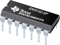
SN55182-SP 抗辐射 V 类双路差动线路驱动器
 The SN55182 dual differential line receiver is designed to sense small differential signals in the presence of large common-mode noise. This device gives TTL-compatible output signals as a function of the polarity of the differential input voltage. The frequency response of each channel can be easily controlled by a single external capacitor to provide immunity to differential noise spikes. The output goes to a high level when the inputs are open circuited. A strobe input (STRB) is provided that, when in the low level, disables the receiver and forces the output to a high level.
The receiver is of monolithic single-chip construction, and both halves of the dual circuits use common power-supply and ground terminals.
The SN55182 is characterized for operation over the full military temperature range of –55°C to 125°C
| SN55182-SP | |
| Operating Temperature Range(�C) | -55 to 125 |
| Pin/Package | 14CDIP, 14CFP |
| Rating | Space |
SN55182-SP 特性
- Single 5-V Supply
- Differential Line Operation
- Dual Channels
- TTL Compatibility
- ±15-V Common-Mode Input Voltage Range
- ±15-V Differential Input Voltage Range
- Individual Channel Strobes
- Built-In Optional Line-Termination Resistor
- Individual Frequency Response Controls
- Designed for Use With Dual Differential Drivers SN55183 and SN75183
- Designed to Be Interchangeable With National Semiconductor DS7820A and DS8820A
- Rad-Tolerant: >40 kRad (Si) ELDRS
- QML-V Qualified, SMD 5962-79008
SN55182-SP 芯片订购指南
| 器件 | 状态 | 温度 | 价格 | 封装 | 引脚 | 封装数量 | 封装载体 | 丝印标记 |
| 5962-7900801VCA | ACTIVE | -55 to 125 | 157.28 | 100u | CDIP (J) | 14 | 1 | TUBE |
SN55182-SP 质量与无铅数据
| 器件 | 环保计划* | 铅/焊球涂层 | MSL 等级/回流焊峰 | 环保信息与无铅 (Pb-free) | DPPM / MTBF / FIT 率 |
| 5962-7900801VCA | TBD | A42 | N/A for Pkg Type | 5962-7900801VCA | 5962-7900801VCA |
SN55182-SP 应用技术支持与电子电路设计开发资源下载
- SN55182-SP 数据资料 dataSheet 下载.PDF
- TI 德州仪器其它接口选型与价格 . xls
- 所选封装材料的热学和电学性质 (PDF 645 KB)
- 使用数字隔离器设计隔离式 I2C 总线接口 (zhct119.PDF, 339 KB)
- 1Q 2011 Issue Analog Applications Journal (slyt399.PDF, 964 KB)
- 接口选择指南 (Rev. D) (PDF 2994 KB)
- Signaling Rate vs. Distance for Differential Buffers (PDF 420 KB)
- Q1 2009 Issue Analog Applications Journal (slyt319.PDF, 1.39 MB)
- Isolated RS-485 Reference Design (PDF 80 KB)
- 无铅组件涂层的保存期评估 (PDF 1305 KB)
- Analog Signal Chain Guide (8.62 MB)
- Industrial Interface IC Solutions (101 KB)
