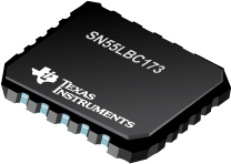
SN55LBC173 四路低功耗差动线路驱动器
 The SN55LBC173 is a monolithic quadruple differential line receiver with 3-state outputs designed to meet the requirements of the EIA standards RS-422-A, RS-423-A, RS-485, and CCITT V.11. This device is optimized for balanced multipoint bus transmission at data rates up to and exceeding 10 million bits per second. The four receivers share two ORed enable inputs, one active when high, the other active when low. Each receiver features high input impedance, input hysteresis for increased noise immunity, and input sensitivity of ±200 mV over a common-mode input voltage range of 12 V to -7 V. Fail-safe design ensures that if the inputs are open circuited, the output is always high. The SN55LBC173 is designed using the Texas Instruments proprietary LinBiCMOSTM technology that provides low power consumption, high switching speeds, and robustness.
|
SN55LBC172 |
SN55LBC173 |
SN65LBC172 |
SN65LBC173 |
SN75LBC172 |
SN75LBC173 |
| Drivers Per Package |
4 |
|
4 |
|
4 |
|
| Receivers Per Package |
|
4 |
|
4 |
|
4 |
| Supply Voltage(s)(V) |
5 |
5 |
5 |
5 |
5 |
5 |
| ESD(kV) |
2 |
2 |
2 |
2 |
2 |
2 |
| Temp Range(C) |
-55 to 125 |
-55 to 125 |
-40 to 85 |
-40 to 85 |
0 to 70 |
0 to 70 |
| Signaling Rate(Mbps) |
10 |
10 |
10 |
10 |
10 |
10 |
| ICC(Max)(mA) |
7 |
11 |
7 |
20 |
7 |
20 |
| Fail Safe |
|
Open |
|
Open |
|
Open |
| Isolated |
No |
No |
No |
No |
No |
No |
| # of TX/RX |
4 TX / 0 RX |
0 TX / 4 RX |
4 TX / 0 RX |
0 TX / 4 RX |
4 TX / 0 RX |
0 TX / 4 RX |
| Common Mode Range |
-7 to 12 |
-7 to 12 |
-7 to 12 |
-7 to 12 |
-7 to 12 |
-7 to 12 |
| Number of Nodes |
32 |
32 |
32 |
32 |
32 |
32 |
| Duplex |
N/A |
N/A |
N/A |
N/A |
N/A |
N/A |
| Footprint |
AM26LS31 |
AM26LS32 |
AM26LS31 |
AM26LS32 |
AM26LS31 |
AM26LS32 |
| Comments |
Upgrade to ALS172A: Lower Power |
Upgrade to ALS173/A: Lower Power |
Upgrade to ALS172A: Lower Power |
Upgrade to ALS173/A: Lower Power |
Upgrade to ALS172A: Lower Power |
Upgrade to ALS173/A: Lower Power |
| Pin/Package |
16CDIP, 16CFP, 20LCCC |
16CDIP, 16CFP, 20LCCC |
16PDIP, 20SOIC |
16PDIP, 16SOIC |
16PDIP, 20SOIC |
16PDIP, 16SOIC |
| Rating |
Military |
Military |
Catalog |
Catalog |
Catalog |
Catalog |
| Fault Protection(V) |
-10 to 15 |
-10 to 15 |
-10 to 15 |
-10 to 15 |
-10 to 15 |
-10 to 15 |
SN55LBC173 特性
- Meets EIA Standards RS-422-A, RS-423-A, RS-485, and CCITT V.11
- Designed to Operate With Pulse Durations as Short as 20 ns
- Designed for Multipoint Bus Transmission on Long Bus Lines in Noisy Environments
- Input Sensitivity...±200 mV
- Low-Power Consumption...20 mA Max
- Open-Circuit Fail-Safe Design
- Pin Compatible With SN75173 and AM26LS32
SN55LBC173 芯片订购指南
| 器件 |
状态 |
温度 |
价格 |
封装 | 引脚 |
封装数量 | 封装载体 |
丝印标记 |
| 5962-9076604Q2A |
ACTIVE |
-55 to 125 |
27.53 | 100u |
LCCC (FK) | 20 |
1 | TUBE |
|
| 5962-9076604QEA |
ACTIVE |
-55 to 125 |
19.88 | 100u |
CDIP (J) | 16 |
1 | TUBE |
|
| 5962-9076604QFA |
ACTIVE |
-55 to 125 |
23.84 | 100u |
CFP (W) | 16 |
1 | TUBE |
|
| SNJ55LBC173FK |
ACTIVE |
-55 to 125 |
27.53 | 100u |
LCCC (FK) | 20 |
1 | TUBE |
|
| SNJ55LBC173J |
ACTIVE |
-55 to 125 |
19.88 | 100u |
CDIP (J) | 16 |
1 | TUBE |
|
| SNJ55LBC173W |
ACTIVE |
-55 to 125 |
23.84 | 100u |
CFP (W) | 16 |
1 | TUBE |
|
SN55LBC173 质量与无铅数据
| 器件 |
环保计划* |
铅/焊球涂层 |
MSL 等级/回流焊峰 |
环保信息与无铅 (Pb-free) |
DPPM / MTBF / FIT 率 |
| 5962-9076604Q2A |
TBD |
POST-PLATE |
N/A for Pkg Type |
5962-9076604Q2A |
5962-9076604Q2A |
| 5962-9076604QEA |
TBD |
A42 |
N/A for Pkg Type |
5962-9076604QEA |
5962-9076604QEA |
| 5962-9076604QFA |
TBD |
A42 |
N/A for Pkg Type |
5962-9076604QFA |
5962-9076604QFA |
| SNJ55LBC173FK |
TBD |
POST-PLATE |
N/A for Pkg Type |
SNJ55LBC173FK |
SNJ55LBC173FK |
| SNJ55LBC173J |
TBD |
A42 |
N/A for Pkg Type |
SNJ55LBC173J |
SNJ55LBC173J |
| SNJ55LBC173W |
TBD |
A42 |
N/A for Pkg Type |
SNJ55LBC173W |
SNJ55LBC173W |
SN55LBC173 应用技术支持与电子电路设计开发资源下载
- SN55LBC173 数据资料 dataSheet 下载.PDF
- TI 德州仪器RS-485选型与价格 . xls
- 所选封装材料的热学和电学性质 (PDF 645 KB)
- 使用数字隔离器设计隔离式 I2C 总线接口 (zhct119.PDF, 339 KB)
- 1Q 2011 Issue Analog Applications Journal (slyt399.PDF, 964 KB)
- 接口选择指南 (Rev. D) (PDF 2994 KB)
- Signaling Rate vs. Distance for Differential Buffers (PDF 420 KB)
- Q1 2009 Issue Analog Applications Journal (slyt319.PDF, 1.39 MB)
- Isolated RS-485 Reference Design (PDF 80 KB)
- 无铅组件涂层的保存期评估 (PDF 1305 KB)
- Analog Signal Chain Guide (8.62 MB)
- Industrial Interface IC Solutions (101 KB)
SN55LBC173 工具和软件
 The SN55LBC173 is a monolithic quadruple differential line receiver with 3-state outputs designed to meet the requirements of the EIA standards RS-422-A, RS-423-A, RS-485, and CCITT V.11. This device is optimized for balanced multipoint bus transmission at data rates up to and exceeding 10 million bits per second. The four receivers share two ORed enable inputs, one active when high, the other active when low. Each receiver features high input impedance, input hysteresis for increased noise immunity, and input sensitivity of ±200 mV over a common-mode input voltage range of 12 V to -7 V. Fail-safe design ensures that if the inputs are open circuited, the output is always high. The SN55LBC173 is designed using the Texas Instruments proprietary LinBiCMOSTM technology that provides low power consumption, high switching speeds, and robustness.