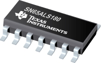
SN65ALS180 差动驱动器和接收器对
 The SN65ALS180 and SN75ALS180 differential driver and receiver pairs are integrated circuits designed for bidirectional data communication on multipoint bus-transmission lines. They are designed for balanced transmission lines and meet TIA/EIA-422-B, TIA/EIA-485-A, and ITU Recommendation V.11.
The SN65ALS180 and SN75ALS180 combine a 3-state differential line driver and a differential input line receiver, both of which operate from a single 5-V power supply. The driver and receiver have active-high and active-low enables, respectively, that can be connected together externally to function as a direction control. The driver differential outputs and the receiver differential inputs are connected to separate terminals for greater flexibility and are designed to offer minimum loading to the bus when the driver is disabled or VCC = 0
|
SN65ALS180 |
| Drivers Per Package |
1 |
| Receivers Per Package |
1 |
| Supply Voltage(s)(V) |
5 |
| ESD(kV) |
2 |
| Temp Range(C) |
-40 to 85 |
| Signaling Rate(Mbps) |
25 |
| ICC(Max)(mA) |
30 |
| Fail Safe |
Open |
| Isolated |
No |
| # of TX/RX |
1 TX / 1 RX |
| Common Mode Range |
-7 to 12 |
| Number of Nodes |
32 |
| Duplex |
Full |
| Footprint |
SN75ALS180 |
| Comments |
Upgrade to Obsolete SN75180: Lower Power |
| Pin/Package |
14SOIC |
| Rating |
Catalog |
| Fault Protection(V) |
-10 to 15 |
SN65ALS180 特性
- Meet or Exceed the Requirements of TIA/EIA-422-B, TIA/EIA-485-A
 and ITU Recommendation V.11
- High-Speed Advanced Low-Power Schottky Circuitry
- Designed for 25-Mbaud Operation in Both Serial and Parallel Applications
- Low Skew Between Devices ...6 ns Max
- Low Supply-Current Requirements . . . 30 mA Max
- Individual Driver and Receiver I/O Pins With Dual VCC and Dual GND
- Wide Positive and Negative Input/Output Bus Voltage Ranges
- Driver Output Capacity . . . ±60 mA
- Thermal Shutdown Protection
- Driver Positive- and Negative-Current Limiting
- Receiver Input Impedance . . . 12 k
 Min
Min
- Receiver Input Sensitivity . . . ±200 mV Max
- Receiver Input Hysteresis . . . 60 mV Typ
- Operate From a Single 5-V Supply
- Glitch-Free Power-Up and Power-Down Protection
SN65ALS180 芯片订购指南
| 器件 |
状态 |
温度 |
价格 |
封装 | 引脚 |
封装数量 | 封装载体 |
丝印标记 |
| SN65ALS180D |
ACTIVE |
-40 to 85 |
2.15 | 1ku |
SOIC (D) | 14 |
50 | TUBE |
|
| SN65ALS180DE4 |
ACTIVE |
-40 to 85 |
2.15 | 1ku |
SOIC (D) | 14 |
50 | TUBE |
|
| SN65ALS180DG4 |
ACTIVE |
-40 to 85 |
2.15 | 1ku |
SOIC (D) | 14 |
50 | TUBE |
|
| SN65ALS180DR |
ACTIVE |
-40 to 85 |
1.80 | 1ku |
SOIC (D) | 14 |
2500 | LARGE T&R |
|
| SN65ALS180DRE4 |
ACTIVE |
-40 to 85 |
1.80 | 1ku |
SOIC (D) | 14 |
2500 | LARGE T&R |
|
| SN65ALS180DRG4 |
ACTIVE |
-40 to 85 |
1.80 | 1ku |
SOIC (D) | 14 |
2500 | LARGE T&R |
|
SN65ALS180 质量与无铅数据
| 器件 |
环保计划* |
铅/焊球涂层 |
MSL 等级/回流焊峰 |
环保信息与无铅 (Pb-free) |
DPPM / MTBF / FIT 率 |
| SN65ALS180D |
Green (RoHS & no Sb/Br) |
CU NIPDAU |
Level-1-260C-UNLIM |
SN65ALS180D |
SN65ALS180D |
| SN65ALS180DE4 |
Green (RoHS & no Sb/Br) |
CU NIPDAU |
Level-1-260C-UNLIM |
SN65ALS180DE4 |
SN65ALS180DE4 |
| SN65ALS180DG4 |
Green (RoHS & no Sb/Br) |
CU NIPDAU |
Level-1-260C-UNLIM |
SN65ALS180DG4 |
SN65ALS180DG4 |
| SN65ALS180DR |
Green (RoHS & no Sb/Br) |
CU NIPDAU |
Level-1-260C-UNLIM |
SN65ALS180DR |
SN65ALS180DR |
| SN65ALS180DRE4 |
Green (RoHS & no Sb/Br) |
CU NIPDAU |
Level-1-260C-UNLIM |
SN65ALS180DRE4 |
SN65ALS180DRE4 |
| SN65ALS180DRG4 |
Green (RoHS & no Sb/Br) |
CU NIPDAU |
Level-1-260C-UNLIM |
SN65ALS180DRG4 |
SN65ALS180DRG4 |
SN65ALS180 应用技术支持与电子电路设计开发资源下载
- SN65ALS180 数据资料 dataSheet 下载.PDF
- TI 德州仪器RS-485选型与价格 . xls
- 所选封装材料的热学和电学性质 (PDF 645 KB)
- 使用数字隔离器设计隔离式 I2C 总线接口 (zhct119.PDF, 339 KB)
- 1Q 2011 Issue Analog Applications Journal (slyt399.PDF, 964 KB)
- 接口选择指南 (Rev. D) (PDF 2994 KB)
- Signaling Rate vs. Distance for Differential Buffers (PDF 420 KB)
- Q1 2009 Issue Analog Applications Journal (slyt319.PDF, 1.39 MB)
- Isolated RS-485 Reference Design (PDF 80 KB)
- 无铅组件涂层的保存期评估 (PDF 1305 KB)
- Analog Signal Chain Guide (8.62 MB)
- Industrial Interface IC Solutions (101 KB)
SN65ALS180 工具和软件
 The SN65ALS180 and SN75ALS180 differential driver and receiver pairs are integrated circuits designed for bidirectional data communication on multipoint bus-transmission lines. They are designed for balanced transmission lines and meet TIA/EIA-422-B, TIA/EIA-485-A, and ITU Recommendation V.11.
 and ITU Recommendation V.11
 Min
Min
