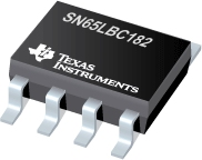
SN65LBC182 半双工、15kV ESD、1/4 UL 收发器
 The SN65LBC182 and SN75LBC182 are differential data line transceivers with a high level of ESD protection in the trade-standard footprint of the SN75176. They are designed for balanced transmission lines and meet ANSI standard TIA/EIA-485-A and ISO 8482. The SN65LBC182 and SN75LBC182 combine a 3-state, differential line driver and differential input line receiver, both of which operate from a single 5-V power supply. The driver and receiver have active-high and active-low enables, respectively, which can be externally connected together to function as a direction control.
The driver outputs and the receiver inputs connect internally to form a differential input/output (I/O) bus port that is designed to offer minimum loading to the bus
|
SN65LBC182 |
| Drivers Per Package |
1 |
| Receivers Per Package |
1 |
| Supply Voltage(s)(V) |
5 |
| ESD(kV) |
15 |
| Temp Range(C) |
-40 to 85 |
| Signaling Rate(Mbps) |
0.25 |
| ICC(Max)(mA) |
30 |
| Fail Safe |
Open |
| Isolated |
No |
| # of TX/RX |
1 TX / 1 RX |
| Common Mode Range |
-7 to 12 |
| Number of Nodes |
128 |
| Duplex |
Half |
| Footprint |
SN75176 |
| Comments |
Similar to LBC184 without Integrated Transient Protection |
| Pin/Package |
8PDIP, 8SOIC |
| Rating |
Catalog |
| Fault Protection(V) |
-10 to 15 |
SN65LBC182 特性
- One-Fourth Unit Load Allows up to 128 Devices on a Bus
- ESD Protection for Bus Terminals:
– ±15-kV Human Body Model
– ±8-kV IEC61000-4-2, Contact Discharge
– ±15-kV IEC61000-4-2, Air-Gap Discharge
- Meets or Exceeds the Requirements of ANSI Standard TIA/EIA-485-A and ISO 8482: 1987(E)
- Controlled Driver Output-Voltage Slew Rates Allow Longer Cable Stub Lengths
- Designed for Signaling Rates† Up to 250-kbps
- Low Disabled Supply Current . . . 250 µA Max
- Thermal Shutdown Protection
- Open-Circuit Fail-Safe Receiver Design
- Receiver Input Hysteresis . . . 70 mV Typ
- Glitch-Free Power-Up and Power-Down Protection
- APPLICATIONS
- Utility Meters
- Industrial Process Control
- Building Automation
SN65LBC182 芯片订购指南
| 器件 |
状态 |
温度 |
价格 |
封装 | 引脚 |
封装数量 | 封装载体 |
丝印标记 |
| SN65LBC182D |
ACTIVE |
-40 to 85 |
2.35 | 1ku |
SOIC (D) | 8 |
75 | TUBE |
|
| SN65LBC182DG4 |
ACTIVE |
-40 to 85 |
2.35 | 1ku |
SOIC (D) | 8 |
75 | TUBE |
|
| SN65LBC182DR |
ACTIVE |
-40 to 85 |
2.00 | 1ku |
SOIC (D) | 8 |
2500 | LARGE T&R |
|
| SN65LBC182DRG4 |
ACTIVE |
-40 to 85 |
2.00 | 1ku |
SOIC (D) | 8 |
2500 | LARGE T&R |
|
| SN65LBC182P |
ACTIVE |
-40 to 85 |
2.35 | 1ku |
PDIP (P) | 8 |
50 | TUBE |
|
| SN65LBC182PE4 |
ACTIVE |
-40 to 85 |
2.35 | 1ku |
PDIP (P) | 8 |
50 | TUBE |
|
SN65LBC182 质量与无铅数据
| 器件 |
环保计划* |
铅/焊球涂层 |
MSL 等级/回流焊峰 |
环保信息与无铅 (Pb-free) |
DPPM / MTBF / FIT 率 |
| SN65LBC182D |
Green (RoHS & no Sb/Br) |
CU NIPDAU |
Level-1-260C-UNLIM |
SN65LBC182D |
SN65LBC182D |
| SN65LBC182DG4 |
Green (RoHS & no Sb/Br) |
CU NIPDAU |
Level-1-260C-UNLIM |
SN65LBC182DG4 |
SN65LBC182DG4 |
| SN65LBC182DR |
Green (RoHS & no Sb/Br) |
CU NIPDAU |
Level-1-260C-UNLIM |
SN65LBC182DR |
SN65LBC182DR |
| SN65LBC182DRG4 |
Green (RoHS & no Sb/Br) |
CU NIPDAU |
Level-1-260C-UNLIM |
SN65LBC182DRG4 |
SN65LBC182DRG4 |
| SN65LBC182P |
Pb-Free (RoHS) |
CU NIPD |
N/A for Pkg Type |
SN65LBC182P |
SN65LBC182P |
| SN65LBC182PE4 |
Pb-Free (RoHS) |
CU NIPD |
N/A for Pkg Type |
SN65LBC182PE4 |
SN65LBC182PE4 |
SN65LBC182 应用技术支持与电子电路设计开发资源下载
- SN65LBC182 数据资料 dataSheet 下载.PDF
- TI 德州仪器RS-485选型与价格 . xls
- 所选封装材料的热学和电学性质 (PDF 645 KB)
- 使用数字隔离器设计隔离式 I2C 总线接口 (zhct119.PDF, 339 KB)
- 1Q 2011 Issue Analog Applications Journal (slyt399.PDF, 964 KB)
- 接口选择指南 (Rev. D) (PDF 2994 KB)
- Signaling Rate vs. Distance for Differential Buffers (PDF 420 KB)
- Q1 2009 Issue Analog Applications Journal (slyt319.PDF, 1.39 MB)
- Isolated RS-485 Reference Design (PDF 80 KB)
- 无铅组件涂层的保存期评估 (PDF 1305 KB)
- Analog Signal Chain Guide (8.62 MB)
- Industrial Interface IC Solutions (101 KB)
SN65LBC182 工具和软件
 The SN65LBC182 and SN75LBC182 are differential data line transceivers with a high level of ESD protection in the trade-standard footprint of the SN75176. They are designed for balanced transmission lines and meet ANSI standard TIA/EIA-485-A and ISO 8482. The SN65LBC182 and SN75LBC182 combine a 3-state, differential line driver and differential input line receiver, both of which operate from a single 5-V power supply. The driver and receiver have active-high and active-low enables, respectively, which can be externally connected together to function as a direction control.