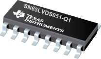
SN65LVDS051-Q1 汽车类高速差动线路驱动器和接收器
The intended application of this device and signaling technique is for point-to-point baseband data transmission over controlled impedance media of approximately 100-Ω characteristic impedance. The transmission media may be printed-circuit board traces, backplanes, or cables
SN65LVDS051-Q1
Input Signal
LVDS, LVTTL
Output Signal
LVDS, LVTTL
No. of Rx
2
No. of Tx
2
Signaling Rate(Mbps)
400
Supply Voltage(s)(V)
3.3
ICC(Max)(mA)
20
Rx tpd(Typ)(ns)
3.7
Tx tpd(Typ)(ns)
1.7
Pin/Package
16SOIC, 16TSSOP
Operating Temperature Range(°C)
-40 to 85
ESD HBM(kV)
2
Approx. Price (US$)
1.60 | 1ku
SN65LVDS051-Q1 特性
Qualified for Automotive Applications
ESD Protection Exceeds 2000 V Per MIL-STD-883, Method 3015; Exceeds 200 V Using Machine Model (C = 200 pF, R = 0)
Meets or Exceeds the Requirements of ANSI TIA/EIA-644-1995 Standard
Signaling Rates up to 400 Mbps
Bus-Terminal ESD Exceeds 12 kV
Operates From a Single 3.3-V Supply
Low-Voltage Differential Signaling With Typical Output Voltages of 350 mV and a 100-Ω Load
Propagation Delay Times
Driver: 1.7 ns Typ
Receiver: 3.7 ns Typ
Power Dissipation at 200 MHz
Driver: 25 mW Typical
Receiver: 60 mW Typical
LVTTL Input Levels Are 5-V Tolerant
Receiver Maintains High Input Impedance With VCC < 1.5 V
Receiver Has Open-Circuit Fail Safe
SN65LVDS051-Q1 芯片订购指南
器件
状态
温度
价格
封装 | 引脚
封装数量 | 封装载体
丝印标记
SN65LVDS051DRG4Q1
ACTIVE
-40 to 85
1.60 | 1ku
SOIC (D) | 16 2500
SN65LVDS051DRQ1
ACTIVE
-40 to 85
1.60 | 1ku
SOIC (D) | 16 2500
SN65LVDS051PWRG4Q1
ACTIVE
-40 to 85
1.60 | 1ku
TSSOP (PW) | 16 2000
SN65LVDS051PWRQ1
ACTIVE
-40 to 85
1.60 | 1ku
TSSOP (PW) | 16 2000
SN65LVDS051-Q1 质量与无铅数据
器件
环保计划*
铅/焊球涂层
MSL 等级/回流焊峰
环保信息与无铅 (Pb-free)
DPPM / MTBF / FIT 率
SN65LVDS051DRG4Q1
Green (RoHS & no Sb/Br)
CU NIPDAU
Level-1-260C-UNLIM
SN65LVDS051DRG4Q1
SN65LVDS051DRG4Q1
SN65LVDS051DRQ1
Green (RoHS & no Sb/Br)
CU NIPDAU
Level-1-260C-UNLIM
SN65LVDS051DRQ1
SN65LVDS051DRQ1
SN65LVDS051PWRG4Q1
Green (RoHS & no Sb/Br)
CU NIPDAU
Level-1-260C-UNLIM
SN65LVDS051PWRG4Q1
SN65LVDS051PWRG4Q1
SN65LVDS051PWRQ1
Green (RoHS & no Sb/Br)
CU NIPDAU
Level-1-260C-UNLIM
SN65LVDS051PWRQ1
SN65LVDS051PWRQ1
SN65LVDS051-Q1 应用技术支持与电子电路设计开发资源下载
SN65LVDS051-Q1 数据资料 dataSheet 下载 .PDF TI 德州仪器LVDS PHYs选型与价格 . xls 所选封装材料的热学和电学性质 (PDF 645 KB)使用数字隔离器设计隔离式 I2C 总线接口 (zhct119.PDF, 339 KB)1Q 2011 Issue Analog Applications Journal (slyt399.PDF, 964 KB)接口选择指南 (Rev. D) (PDF 2994 KB)Signaling Rate vs. Distance for Differential Buffers (PDF 420 KB)Q1 2009 Issue Analog Applications Journal (slyt319.PDF, 1.39 MB)Isolated RS-485 Reference Design (PDF 80 KB)无铅组件涂层的保存期评估 (PDF 1305 KB)Analog Signal Chain Guide (8.62 MB)Industrial Interface IC Solutions (101 KB)
 The SN65LVDS179, SN65LVDS180, SN65LVDS050, and SN65LVDS051 are differential line drivers and receivers that use low-voltage differential signaling (LVDS) to achieve signaling rates as high as 400 Mbps. The TIA/EIA-644 standard compliant electrical interface provides a minimum differential output voltage magnitude of 247 mV into a 100-Ω load and receipt of 50-mV signals with up to 1 V of ground potential difference between a transmitter and receiver.
