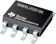
SN65LVDS100 2Gbps LVDS/LVPECL/CML 至 LVDS 中继器/转换器
 The SN65LVDS100, SN65LVDT100, SN65LVDS101, and SN65LVDT101 are a high-speed differential receiver and driver connected as a repeater. The receiver accepts low-voltage differential signaling (LVDS), positive-emitter-coupled logic (PECL), or current-mode logic (CML) input signals at rates up to 2 Gbps and repeats it as either an LVDS or PECL output signal. The signal path through the device is differential for low radiated emissions and minimal added jitter.
The outputs of the SN65LVDS100 and SN65LVDT100 are LVDS levels as defined by TIA/EIA-644-A. The outputs of the SN65LVDS101 and SN65LVDT101 are compatible with 3.3-V PECL levels. Both drive differential transmission lines with nominally 100- characteristic impedance
|
SN65CML100 |
SN65LVDS100 |
SN65LVDS101 |
SN65LVDS16 |
SN65LVDS17 |
SN65LVDS18 |
SN65LVDS19 |
SN65LVDS20 |
SN65LVP16 |
SN65LVP17 |
SN65LVP18 |
SN65LVP19 |
SN65LVP20 |
| Supply Voltage(s)(V) |
3.3 |
3.3 |
3.3 |
2.5 , 3.3 |
2.5 , 3.3 |
2.5 , 3.3 |
2.5 , 3.3 |
2.5 , 3.3 |
2.5 , 3.3 |
2.5 , 3.3 |
2.5 , 3.3 |
2.5 , 3.3 |
2.5 , 3.3 |
| ICC(Max)(mA) |
12 |
30 |
90 |
48 |
48 |
36 |
36 |
45 |
48 |
48 |
36 |
36 |
45 |
| Signaling Rate(Mbps) |
1500 |
2000 |
2000 |
4000 |
4000 |
2000 |
2000 |
4000 |
4000 |
4000 |
4000 |
2000 |
4000 |
| No. of Tx |
1 |
1 |
1 |
1 |
1 |
1 |
1 |
1 |
1 |
1 |
1 |
1 |
1 |
| Operating Temperature Range(�C) |
-40 to 85 |
-40 to 85 |
-40 to 85 |
-40 to 85 |
-40 to 85 |
-40 to 85 |
-40 to 85 |
-40 to 85 |
-40 to 85 |
-40 to 85 |
-40 to 85 |
-40 to 85 |
-40 to 85 |
| Tx tpd(Typ)(ns) |
|
|
|
0.460 |
0.460 |
0.460 |
0.460 |
0.450 |
0.460 |
0.460 |
0.460 |
0.460 |
0.450 |
| No. of Rx |
1 |
1 |
1 |
1 |
1 |
1 |
1 |
1 |
1 |
1 |
1 |
1 |
1 |
| Input Signal |
CML, LVDS, LVPECL |
CML, LVDS, LVPECL |
CML, LVDS, LVPECL |
Single-Ended |
Differential |
Single-Ended |
Differential |
Differential |
Single-Ended |
Differential |
Single-Ended |
Differential |
Differential |
| Rx tpd(Typ)(ns) |
0.8 |
0.8 |
0.9 |
|
|
|
|
0.630 |
|
|
|
|
0.630 |
| Output Signal |
CML |
LVDS |
LVPECL |
LVDS |
LVDS |
LVDS |
LVDS |
LVDS |
LVPECL |
LVPECL |
LVPECL |
LVPECL |
LVPECL |
| Peak-to-Peak Jitter(Max)(ps) |
70 |
65 |
61 |
|
|
|
|
35 |
|
|
|
|
35 |
| Part-to-Part Skew(Max)(ps) |
100 |
100 |
100 |
80 |
80 |
80 |
80 |
80 |
80 |
80 |
80 |
80 |
80 |
| ESD HBM(kV) |
5 |
5 |
5 |
3 |
3 |
3 |
3 |
3 |
3 |
3 |
3 |
3 |
3 |
| Pin/Package |
8MSOP, 8SOIC |
8MSOP, 8SOIC |
8MSOP, 8SOIC |
8WSON |
8WSON |
8WSON |
8WSON |
8WSON |
8WSON |
8WSON |
8WSON |
8WSON |
8WSON |
SN65LVDS100 特性
- Designed for Signaling Rates(1) ≥ 2 Gbps
- Total Jitter < 65 ps
- Low-Power Alternative for the MC100EP16
- Low 100 ps (Max) Part-To-Part Skew
- 25 mV of Receiver Input Threshold Hysteresis Over 0-V to 4-V Common-Mode Range
- Inputs Electrically Compatible With LVPECL, CML, and LVDS Signal Levels
- 3.3-V Supply Operation
- LVDT Integrates 110-
 Terminating Resistor
- Offered in SOIC and MSOP
- APPLICATIONS
- 622 MHz Central Office Clock Distribution
- High-Speed Network Routing
- Wireless Basestations
- Low Jitter Clock Repeater
- Serdes LVPECL Output to FPGA LVDS Input Translator
SN65LVDS100 芯片订购指南
| 器件 |
状态 |
温度 |
价格 |
封装 | 引脚 |
封装数量 | 封装载体 |
丝印标记 |
| SN65LVDS100D |
ACTIVE |
-40 to 85 |
1.80 | 1ku |
SOIC (D) | 8 |
75 | TUBE |
|
| SN65LVDS100DG4 |
ACTIVE |
-40 to 85 |
1.80 | 1ku |
SOIC (D) | 8 |
75 | TUBE |
|
| SN65LVDS100DR |
ACTIVE |
-40 to 85 |
1.50 | 1ku |
SOIC (D) | 8 |
2500 | LARGE T&R |
|
| SN65LVDS100DRG4 |
ACTIVE |
-40 to 85 |
1.50 | 1ku |
SOIC (D) | 8 |
2500 | LARGE T&R |
|
SN65LVDS100 质量与无铅数据
| 器件 |
环保计划* |
铅/焊球涂层 |
MSL 等级/回流焊峰 |
环保信息与无铅 (Pb-free) |
DPPM / MTBF / FIT 率 |
| SN65LVDS100D |
Pb-Free (RoHS) |
CU NIPDAU |
Level-1-260C-UNLIM |
SN65LVDS100D |
SN65LVDS100D |
| SN65LVDS100DG4 |
Pb-Free (RoHS) |
CU NIPDAU |
Level-1-260C-UNLIM |
SN65LVDS100DG4 |
SN65LVDS100DG4 |
| SN65LVDS100DR |
Pb-Free (RoHS) |
CU NIPDAU |
Level-1-260C-UNLIM |
SN65LVDS100DR |
SN65LVDS100DR |
| SN65LVDS100DRG4 |
Pb-Free (RoHS) |
CU NIPDAU |
Level-1-260C-UNLIM |
SN65LVDS100DRG4 |
SN65LVDS100DRG4 |
SN65LVDS100 应用技术支持与电子电路设计开发资源下载
- SN65LVDS100 数据资料 dataSheet 下载.PDF
- TI 德州仪器转发器/转换器选型与价格 . xls
- 所选封装材料的热学和电学性质 (PDF 645 KB)
- 使用数字隔离器设计隔离式 I2C 总线接口 (zhct119.PDF, 339 KB)
- 1Q 2011 Issue Analog Applications Journal (slyt399.PDF, 964 KB)
- 接口选择指南 (Rev. D) (PDF 2994 KB)
- Signaling Rate vs. Distance for Differential Buffers (PDF 420 KB)
- Q1 2009 Issue Analog Applications Journal (slyt319.PDF, 1.39 MB)
- Isolated RS-485 Reference Design (PDF 80 KB)
- 无铅组件涂层的保存期评估 (PDF 1305 KB)
- Analog Signal Chain Guide (8.62 MB)
- Industrial Interface IC Solutions (101 KB)
SN65LVDS100 工具和软件
 The SN65LVDS100, SN65LVDT100, SN65LVDS101, and SN65LVDT101 are a high-speed differential receiver and driver connected as a repeater. The receiver accepts low-voltage differential signaling (LVDS), positive-emitter-coupled logic (PECL), or current-mode logic (CML) input signals at rates up to 2 Gbps and repeats it as either an LVDS or PECL output signal. The signal path through the device is differential for low radiated emissions and minimal added jitter.
![]() characteristic impedance
characteristic impedance Terminating Resistor

