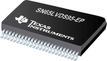
SN65LVDS95-EP 增强型产品 Lvds Serdes 发送器
 The SN65LVDS95 LVDS serdes (serializer/deserializer) transmitter contains three 7-bit parallel-load serial-out shift registers, a 7× clock synthesizer, and four low-voltage differential signaling (LVDS) line drivers in a single integrated circuit. These functions allow 21 bits of single-ended LVTTL data to be synchronously transmitted over 4 balanced-pair conductors for receipt by a compatible receiver, such as the SN65LVDS96.
When transmitting, data bits D0 through D20 are each loaded into registers of the SN65LVDS95 on the rising edge of the input clock signal (CLKIN). The frequency of CLKIN is multiplied seven times and then used to serially unload the data registers in 7-bit slices. The three serial streams and a phase-locked clock (CLKOUT) are then output to LVDS output drivers
|
SN65LVDS95-EP |
| Data Throughput(MB/s) |
170.625 |
| Number of Parallel Inputs |
21 |
| Serial Data Transmitter Channels |
3 |
| PLL Frequency(MHz) |
20 - 68 |
| ICC(mA) |
110 |
| Supply Voltage(s)(V) |
3.3 |
| Pin/Package |
48TSSOP |
| Footprint |
SN65LVDS85 |
| Operating Temperature Range(C) |
-40 to 85 |
| Type of Line Circuit |
LVDS |
SN65LVDS95-EP 特性
- Controlled Baseline
- One Assembly/Test Site, One Fabrication Site
- Enhanced Diminishing Manufacturing
Sources (DMS) Support
- Enhanced Product-Change Notification
- Qualification Pedigree

- 21:3 Data Channel Compression at up to
1.36 Gigabits per Second Throughput
- Suited for Point-to-Point Subsystem
Communication With Very Low EMI
- 21 Data Channels Plus Clock in
Low-Voltage TTL and 3 Data Channels Plus
Clock Out Low-Voltage Differential
- Operates From a Single 3.3-V Supply and
250 mW (Typ)
- 5-V Tolerant Data Inputs
- ’LVDS95 Has Rising Clock Edge Triggered Inputs
- Bus Pins Tolerate 6-kV HBM ESD
- Packaged in Thin Shrink Small-Outline
Package With 20 Mil Terminal Pitch
- Consumes <1 mW When Disabled
- Wide Phase-Lock Input Frequency Range
20 MHz to 68 MHz
- No External Components Required for PLL
- Inputs Meet or Exceed the Requirements of
ANSI EIA/TIA-644 Standard
- Industrial Temperature Qualified
TA = –40°C to 85°C
- Replacement for the National DS90CR215
SN65LVDS95-EP 芯片订购指南
| 器件 |
状态 |
温度 |
价格 |
封装 | 引脚 |
封装数量 | 封装载体 |
丝印标记 |
| SN65LVDS95DGGREP |
ACTIVE |
-40 to 85 |
4.40 | 100u |
TSSOP (DGG) | 48 |
2000 | LARGE T&R |
|
| V62/04643-01XE |
ACTIVE |
-40 to 85 |
4.40 | 100u |
TSSOP (DGG) | 48 |
2000 | LARGE T&R |
|
SN65LVDS95-EP 质量与无铅数据
| 器件 |
环保计划* |
铅/焊球涂层 |
MSL 等级/回流焊峰 |
环保信息与无铅 (Pb-free) |
DPPM / MTBF / FIT 率 |
| SN65LVDS95DGGREP |
Green (RoHS & no Sb/Br) |
CU NIPDAU |
Level-2-260C-1 YEAR |
SN65LVDS95DGGREP |
SN65LVDS95DGGREP |
| V62/04643-01XE |
Green (RoHS & no Sb/Br) |
CU NIPDAU |
Level-2-260C-1 YEAR |
V62/04643-01XE |
V62/04643-01XE |
SN65LVDS95-EP 应用技术支持与电子电路设计开发资源下载
- SN65LVDS95-EP 数据资料 dataSheet 下载.PDF
- TI 德州仪器串行器和解串器选型与价格 . xls
- 所选封装材料的热学和电学性质 (PDF 645 KB)
- 使用数字隔离器设计隔离式 I2C 总线接口 (zhct119.PDF, 339 KB)
- 高性能SERDES及其在CPRI 接口的应用分析 (zhca076.HTM, 8 KB)
- 1Q 2011 Issue Analog Applications Journal (slyt399.PDF, 964 KB)
- 接口选择指南 (Rev. D) (PDF 2994 KB)
- Signaling Rate vs. Distance for Differential Buffers (PDF 420 KB)
- Q1 2009 Issue Analog Applications Journal (slyt319.PDF, 1.39 MB)
- Isolated RS-485 Reference Design (PDF 80 KB)
- 无铅组件涂层的保存期评估 (PDF 1305 KB)
- Analog Signal Chain Guide (8.62 MB)
- Industrial Interface IC Solutions (101 KB)
 The SN65LVDS95 LVDS serdes (serializer/deserializer) transmitter contains three 7-bit parallel-load serial-out shift registers, a 7× clock synthesizer, and four low-voltage differential signaling (LVDS) line drivers in a single integrated circuit. These functions allow 21 bits of single-ended LVTTL data to be synchronously transmitted over 4 balanced-pair conductors for receipt by a compatible receiver, such as the SN65LVDS96.
