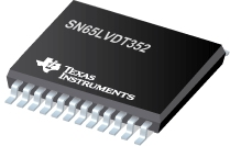
SN65LVDT352 具有 -4 至 5V 共模范围的双路 LVDS 接收器
SN65LVDT352
Input Signal
CMOS, ECL, LVCMOS, LVDS, LVECL, LVPECL, PECL
Output Signal
LVTTL
No. of Rx
4
No. of Tx
560
Signaling Rate(Mbps)
3.3
Rx tpd(Typ)(ns)
20
Tx tpd(Typ)(ns)
4
Part-to-Part Skew(Max)(ps)
1000
Pin/Package
24TSSOP
Operating Temperature Range(°C)
-40 to 85
ESD HBM(kV)
15
Approx. Price (US$)
2.00 | 1ku
SN65LVDT352 特性
Meets or Exceeds the Requirements of ANSI TIA/EIA-644A Standard
Single-Channel Signaling Rates1 up to 560 Mbps
–4 V to 5 V Common-Mode Input Voltage Range
Flow-Through Architecture
Active Failsafe Assures a High-level Output When an Input Signal Is not Present
SN65LVDS348 Provides a Wide Common-Mode Range Replacement for the SN65LVDS048A or the DS90LV048A
APPLICATIONS
Logic Level Translator
Point-to-Point Baseband Data Transmission Over 100- ECL/PECL-to-LVTTL Conversion
Wireless Base Stations
Central Office or PABX Switches
SN65LVDT352 芯片订购指南
器件
状态
温度
价格
封装 | 引脚
封装数量 | 封装载体
丝印标记
SN65LVDT352PW
ACTIVE
-40 to 85
2.40 | 1ku
TSSOP (PW) | 24 60 | TUBE
SN65LVDT352PWG4
ACTIVE
-40 to 85
2.40 | 1ku
TSSOP (PW) | 24 60 | TUBE
SN65LVDT352PWR
ACTIVE
-40 to 85
2.00 | 1ku
TSSOP (PW) | 24 2000 | LARGE T&R
SN65LVDT352PWRG4
ACTIVE
-40 to 85
2.00 | 1ku
TSSOP (PW) | 24 2000 | LARGE T&R
SN65LVDT352 质量与无铅数据
器件
环保计划*
铅/焊球涂层
MSL 等级/回流焊峰
环保信息与无铅 (Pb-free)
DPPM / MTBF / FIT 率
SN65LVDT352PW
Green (RoHS & no Sb/Br)
CU NIPDAU
Level-2-260C-1 YEAR
SN65LVDT352PW
SN65LVDT352PW
SN65LVDT352PWG4
Green (RoHS & no Sb/Br)
CU NIPDAU
Level-2-260C-1 YEAR
SN65LVDT352PWG4 SN65LVDT352PWG4
SN65LVDT352PWR
Green (RoHS & no Sb/Br)
CU NIPDAU
Level-2-260C-1 YEAR
SN65LVDT352PWR
SN65LVDT352PWR
SN65LVDT352PWRG4
Green (RoHS & no Sb/Br)
CU NIPDAU
Level-2-260C-1 YEAR
SN65LVDT352PWRG4 SN65LVDT352PWRG4
SN65LVDT352 应用技术支持与电子电路设计开发资源下载
SN65LVDT352 数据资料 dataSheet 下载 .PDF TI 德州仪器LVDS PHYs选型与价格 . xls 所选封装材料的热学和电学性质 (PDF 645 KB)使用数字隔离器设计隔离式 I2C 总线接口 (zhct119.PDF, 339 KB)1Q 2011 Issue Analog Applications Journal (slyt399.PDF, 964 KB)接口选择指南 (Rev. D) (PDF 2994 KB)Signaling Rate vs. Distance for Differential Buffers (PDF 420 KB)Q1 2009 Issue Analog Applications Journal (slyt319.PDF, 1.39 MB)Isolated RS-485 Reference Design (PDF 80 KB)无铅组件涂层的保存期评估 (PDF 1305 KB)Analog Signal Chain Guide (8.62 MB)Industrial Interface IC Solutions (101 KB)
 The SN65LVDS348, SN65LVDT348, SN65LVDS352, and SN65LVDT352 are high-speed, quadruple differential receivers with a wide common-mode input voltage range. This allows receipt of TIA/EIA-644 signals with up to 3-V of ground noise or a variety of differential and single-ended logic levels. The ’348 is in a 16-pin package to match the industry-standard footprint of the DS90LV048. The ’352 adds two additional VCC and GND pins in a 24-pin package to provide higher data transfer rates with multiple receivers in operation. All offer a flow-through architecture with all inputs on one side and outputs on the other to ease board layout and reduce crosstalk between receivers. LVDT versions of both integrate a 110-
![]() line termination resistor.
line termination resistor. Media
Media

