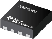
SN65MLVD3 Single M-LVDS Receivers
The M-LVDS standard defines two types of receivers, designated as Type-1 and Type-2. Type-1 receivers (SN65MLVD2) have thresholds centered about zero with 25 mV of hysteresis to prevent output oscillations with loss of input; Type-2 receivers (SN65MLVD3) implement a failsafe by using an offset threshold. Receiver outputs are slew rate controlled to reduce EMI and crosstalk effects associated with large current surges
SN65MLVD2 SN65MLVD301 SN65MLVD3
No. of Rx
1
1
1
No. of Tx
1
Input Signal
M-LVDS
LVTTL, M-LVDS
M-LVDS
Output Signal
LVTTL
LVTTL, M-LVDS
LVTTL
Signaling Rate(Mbps)
250
200
250
Supply Voltage(s)(V)
3.3
3.3
3.3
ICC(Max)(mA)
25
24
25
Receiver Type
1
1
2
Peak-to-Peak Jitter(Max)(ps)
10
8
Part-to-Part Skew(Max)(ps)
100
1000
100
Rx tpd(Typ)(ns)
6
4
6
Tx tpd(Typ)(ns)
1.5
Pin/Package
8SON
8SOIC
8SON
Operating Temperature Range(�C)
-40 to 85
-40 to 85
-40 to 85
ESD HBM(kV)
8
8
8
SN65MLVD3 特性
Low-Voltage Differential 30- SN65MLVD3 Type-1 Receiver Incorporates 25 mV of Input Threshold Hysteresis
SN65MLVD3 Type-2 Receiver Provides 100 mV Offset Threshold to Detect Open-Circuit and Idle-Bus Conditions
Wide Receiver Input Common-Mode Voltage Range, -1 V to 3.4 V, Allows 2 V of Ground Noise
Improved VIT (35 mV)
Meets or Exceeds the M-LVDS Standard TIA/EIA-899 for Multipoint Topology
High Input Impedance with Low Supply Voltage
Bus-Pin HBM ESD Protection Exceeds 9 kV
Packaged in 8-Pin SON (DRB) 70% Smaller Than 8-Pin SOIC
APPLICATIONS
Parallel Multipoint Data and Clock Transmission via Backplanes and Cables
Cellular Base Stations
Central Office Switches
Network Switches and Routers
SN65MLVD3 芯片订购指南
器件
状态
温度
价格
封装 | 引脚
封装数量 | 封装载体
丝印标记
SN65MLVD3DRBR
ACTIVE
-40 to 85
0.90 | 1ku
SON (DRB) | 8 3000 | LARGE T&R
SN65MLVD3DRBRG4
ACTIVE
-40 to 85
0.90 | 1ku
SON (DRB) | 8 3000 | LARGE T&R
SN65MLVD3DRBT
ACTIVE
-40 to 85
1.05 | 1ku
SON (DRB) | 8 250 | SMALL T&R
SN65MLVD3DRBTG4
ACTIVE
-40 to 85
1.05 | 1ku
SON (DRB) | 8 250 | SMALL T&R
SN65MLVD3 质量与无铅数据
器件
环保计划*
铅/焊球涂层
MSL 等级/回流焊峰
环保信息与无铅 (Pb-free)
DPPM / MTBF / FIT 率
SN65MLVD3DRBR
Green (RoHS & no Sb/Br)
CU NIPDAU
Level-2-260C-1 YEAR
SN65MLVD3DRBR
SN65MLVD3DRBR
SN65MLVD3DRBRG4
Green (RoHS & no Sb/Br)
CU NIPDAU
Level-2-260C-1 YEAR
SN65MLVD3DRBRG4 SN65MLVD3DRBRG4
SN65MLVD3DRBT
Green (RoHS & no Sb/Br)
CU NIPDAU
Level-2-260C-1 YEAR
SN65MLVD3DRBT
SN65MLVD3DRBT
SN65MLVD3DRBTG4
Green (RoHS & no Sb/Br)
CU NIPDAU
Level-2-260C-1 YEAR
SN65MLVD3DRBTG4 SN65MLVD3DRBTG4
SN65MLVD3 应用技术支持与电子电路设计开发资源下载
SN65MLVD3 数据资料 dataSheet 下载 .PDF TI 德州仪器M-LVDS PHYs选型与价格 . xls 所选封装材料的热学和电学性质 (PDF 645 KB)使用数字隔离器设计隔离式 I2C 总线接口 (zhct119.PDF, 339 KB)1Q 2011 Issue Analog Applications Journal (slyt399.PDF, 964 KB)接口选择指南 (Rev. D) (PDF 2994 KB)Signaling Rate vs. Distance for Differential Buffers (PDF 420 KB)Q1 2009 Issue Analog Applications Journal (slyt319.PDF, 1.39 MB)Isolated RS-485 Reference Design (PDF 80 KB)无铅组件涂层的保存期评估 (PDF 1305 KB)Analog Signal Chain Guide (8.62 MB)Industrial Interface IC Solutions (101 KB)
SN65MLVD3 工具和软件
 The SN65MLVD2 and SN65MLVD3 are single-channel M-LVDS receivers. These devices are designed in full compliance with the TIA/EIA-899 (M-LVDS) standard, which are optimized to operate at signaling rates up to 250 Mbps. Each receiver channel is controlled by a receive enable (RE). When RE = low, the corresponding channel is enabled; when RE = high, the corresponding channel is disabled.
 Line Receivers for Signaling Rates(1) up to 250Mbps; Clock Frequencies up to 125MHz

