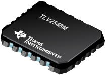
TLV2548M 12 位 200kSPS ADC,具有串行 输出、自动断电(软件和硬件)、低功耗、8 x FIFO 和 8 通道
 The TLV2544Q, TLV2548Q, and TLV2548M are a family of high performance, 12-bit low power, 3.5 µs, CMOS analog-to-digital converters (ADC) which operate from a single 3-V to 5.5-V power supply. These devices have three digital inputs and a 3-state output [chip select (CS), serial input-output clock (SCLK), serial data input (SDI), and serial data output (SDO)] that provide a direct 4-wire interface to the serial port of most popular host microprocessors (SPI interface). When interfaced with a DSP, a frame sync (FS) signal is used to indicate the start of a serial data frame.
In addition to a high-speed A/D converter and versatile control capability, these devices have an on-chip analog multiplexer that can select any analog inputs or one of three internal self-test voltages
|
TLV2548M |
| # Input Channels |
8 |
| Interface |
Serial SPI Interface |
| Input Range |
+2V, +4V |
| Architecture |
SAR |
| Rating |
Military |
| Operating Temperature Range (C) |
-55 to 125 |
| Pin/Package |
20LCCC |
TLV2548M 特性
- Maximum Throughput 200-KSPS
- Built-In Reference, Conversion Clock and 8× FIFO
- Differential/Integral Nonlinearity Error:
±1.2 LSB at –55°C to 125°C
- Signal-to-Noise and Distortion Ratio:
65 dB, fi = 12-kHz at –55°C to 125°C
- Spurious Free Dynamic Range: 75 dB, fi = 12- kHz
- SPI/DSP-Compatible Serial Interfaces With SCLK up to 20-MHz
- Single Wide Range Supply 3 Vdc to 5.5 Vdc
- Analog Input Range 0-V to Supply Voltage With 500 kHz BW
- Hardware Controlled and Programmable Sampling Period
- Low Operating Current (1-mA at 3.3-V, 2-mA at 5.5-V With External Ref,
1.7-mA at 3.3-V, 2.4-mA at 5.5-V With Internal Ref)
- Power Down: Software/Hardware Power-Down Mode (1 µA Typ, Ext Ref),
Autopower-Down Mode (1 µA Typ, Ext Ref)
- Programmable Auto-Channel Sweep
- Available in Q-Temp Automotive High Reliability Automotive Applications
Configuration Control/Print Support Qualification to Automotive Standards
TLV2548M 芯片订购指南
| 器件 |
状态 |
温度 (oC) |
价格(美元) |
封装 | 引脚 |
封装数量 | 封装载体 |
丝印标记 |
| 5962-9957001Q2A |
ACTIVE |
-55 to 125 |
209.61 | 1ku |
LCCC (FK) | 20 |
1 | TUBE |
|
| TLV2548MFKB |
ACTIVE |
-55 to 125 |
209.61 | 1ku |
LCCC (FK) | 20 |
1 | TUBE |
|
TLV2548M 质量与无铅数据
| 器件 |
环保计划* |
铅/焊球涂层 |
MSL 等级/回流焊峰 |
环保信息与无铅 (Pb-free) |
DPPM / MTBF / FIT 率 |
| 5962-9957001Q2A |
TBD |
Call TI |
Call TI |
5962-9957001Q2A |
5962-9957001Q2A |
| TLV2548MFKB |
TBD |
POST-PLATE |
N/A for Pkg Type |
TLV2548MFKB |
TLV2548MFKB |
TLV2548M 工具与软件
TLV2548M 应用技术支持与电子电路设计开发资源下载
- TLV2548M 数据资料 dataSheet 下载.PDF
- TI 德州仪器数据转换器选型与价格参考 . xls
- Determining Minimum Acquisition Times for SAR ADCs, part 2
- Determining Minimum Acquisition Times for SAR ADCs, part 1
 The TLV2544Q, TLV2548Q, and TLV2548M are a family of high performance, 12-bit low power, 3.5 µs, CMOS analog-to-digital converters (ADC) which operate from a single 3-V to 5.5-V power supply. These devices have three digital inputs and a 3-state output [chip select (CS), serial input-output clock (SCLK), serial data input (SDI), and serial data output (SDO)] that provide a direct 4-wire interface to the serial port of most popular host microprocessors (SPI interface). When interfaced with a DSP, a frame sync (FS) signal is used to indicate the start of a serial data frame.