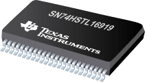
SN74HSTL16919 具有输入上拉电阻的 9 位至 18 位 HSTL 到 LVTTL 存储器地址锁存器
 This 9-bit to 18-bit D-type latch is designed for 3.15-V to 3.45-V VCC operation. The D inputs accept HSTL levels and the Q outputs provide LVTTL levels.
The SN74HSTL16919 is particularly suitable for driving an address bus to two banks of memory. Each bank of nine outputs is controlled with its own latch-enable (LE\) input.
Each of the nine D inputs is tied to the inputs of two D-type latches that provide true data (Q) at the outputs. While LE\ is low, the Q outputs of the corresponding nine latches follow the D inputs. When LE\ is taken high, the Q outputs are latched at the levels set up at the D inputs.
To ensure low ICC during power up or power down, 10-k![]() pullup resistors are included on the D and (LE )\inputs to ensure a differential voltage relative to VREF
pullup resistors are included on the D and (LE )\inputs to ensure a differential voltage relative to VREF
| SN74HSTL16919 | |
| Voltage Nodes(V) | 3.3, 2.5 |
| Technology Family | SSTL |
| Rating | Catalog |
SN74HSTL16919 特性
- Member of the Texas Instruments WidebusTM Family
- Supports SSTL_3 Signal Inputs and Outputs
- Flow-Through Architecture Optimizes PCB Layout
- Meets SSTL_3 Class I and Class II Specifications
- Latch-Up Performance Exceeds 250 mA Per JESD 17
- Packaged in Plastic Thin Shrink Small-Outline Package
SN74HSTL16919 芯片订购指南
| 器件 | 状态 | 温度 | 价格(美元) | 封装 | 引脚 | 封装数量 | 封装载体 | 丝印标记 |
| 74SSTL16837ADGGRE4 | ACTIVE | 0 to 70 | 8.25 | 1ku | TSSOP (DGG) | 48 | 2000 | LARGE T&R | |
| 74SSTL16837ADGGRG4 | ACTIVE | 0 to 70 | 8.25 | 1ku | TSSOP (DGG) | 48 | 2000 | LARGE T&R | |
| SN74SSTL16837ADGGR | ACTIVE | 0 to 70 | 8.25 | 1ku | TSSOP (DGG) | 48 | 2000 | LARGE T&R |
SN74HSTL16919 质量与无铅数据
| 器件 | 环保计划* | 铅/焊球涂层 | MSL 等级/回流焊峰 | 环保信息与无铅 (Pb-free) | DPPM / MTBF / FIT 率 |
| 74SSTL16837ADGGRE4 | Green (RoHS & no Sb/Br) | CU NIPDAU | Level-1-260C-UNLIM | 74SSTL16837ADGGRE4 | 74SSTL16837ADGGRE4 |
| 74SSTL16837ADGGRG4 | Green (RoHS & no Sb/Br) | CU NIPDAU | Level-1-260C-UNLIM | 74SSTL16837ADGGRG4 | 74SSTL16837ADGGRG4 |
| SN74SSTL16837ADGGR | Green (RoHS & no Sb/Br) | CU NIPDAU | Level-1-260C-UNLIM | SN74SSTL16837ADGGR | SN74SSTL16837ADGGR |
SN74HSTL16919 应用技术支持与电子电路设计开发资源下载
- SN74HSTL16919 数据资料 dataSheet 下载.PDF
- TI 德州仪器特殊逻辑产品选型与价格 . xls
- Shelf-Life Evaluation of Lead-Free Component Finishes (PDF 1305 KB)
- Understanding and Interpreting Standard-Logic Data Sheets (PDF 857 KB)
- TI IBIS File Creation, Validation, and Distribution Processes (PDF 380 KB)
- Implications of Slow or Floating CMOS Inputs (PDF 101 KB)
- CMOS Power Consumption and CPD Calculation (PDF 89 KB)
- Designing With Logic (PDF 186 KB)
- Live Insertion (PDF 150 KB)
- Input and Output Characteristics of Digital Integrated Circuits (PDF 1708 KB)
- Using High Speed CMOS and Advanced CMOS in Systems With Multiple Vcc (PDF 43 KB)
- HiRel Unitrode Power Management Brochure (PDF 206 KB)
- LOGIC Pocket Data Book (PDF 6001 KB)
- HiRel Unitrode Power Management Brochure (PDF 206 KB)
- Logic Cross-Reference (PDF 2938 KB)
