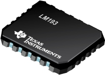
LM193 双路差动比较器

These devices consist of two independent voltage comparators that are designed to operate from a single power supply over a wide range of voltages. Operation from dual supplies also is possible as long as the difference between the two supplies is 2 V to 36 V, and VCC is at least 1.5 V more positive than the input common-mode voltage. Current drain is independent of the supply voltage. The outputs can be connected to other open-collector outputs to achieve wired-AND relationships.
The LM193 is characterized for operation from –55°C to 125°C. The LM293 and LM293A are characterized for operation from –25°C to 85°C. The LM393 and LM393A are characterized for operation from 0°C to 70°C
�
|
LM193 |
| Number of Channels |
4 |
| Iq per channel (Max) (mA) |
0.5 |
| Output Current (Min) (mA) |
6 |
| tRESP Low - to - High (us) |
0.3 |
| Output Type |
Open Collector, Open Drain |
| VIO (25 deg C) (Max) (mV) |
5 |
| Pin/Package |
20LCCC, 8CDIP, 8SOIC |
| VICR (Max) (V) |
3.5 |
| Vs (Min) (V) |
2 |
| Vs (Max) (V) |
36 |
| Operating Temperature Range (C) |
-55 to 125 |
| Rating |
Military |
LM193 特性
- Single Supply or Dual Supplies
- Wide Range of Supply Voltage...2 V to 36 V
- Max Rating . . . 2 V to 36 V
- Tested to 30 V… Non-V Devices
- Tested to 32 V… V-Suffix Devices
- Low Supply-Current Drain Independent of Supply Voltage . . . 0.4 mA Typ Per Comparator
- Low Input Bias Current . . . 25 nA Typ
- Low Input Offset Current ...3 nA Typ (LM193)
- Low Input Offset Voltage ...2 mV Typ
- Common-Mode Input Voltage Range Includes Ground
- Differential Input Voltage Range Equal to Maximum-Rated Supply Voltage . . . ±36 V
- Low Output Saturation Voltage
- Output Compatible With TTL, MOS, and CMOS
LM193 芯片订购指南
| 器件 |
状态 |
温度 |
价格(美元) |
封装 | 引脚 |
封装数量 | 封装载体 |
丝印标记 |
| 5962-9452601Q2A |
ACTIVE |
-55 to 125 |
9.34 | 1ku |
LCCC (FK) | 20 |
1 | TUBE |
|
| 5962-9452601QPA |
ACTIVE |
-55 to 125 |
3.09 | 1ku |
CDIP (JG) | 8 |
1 | TUBE |
|
| JM38510/11202BPA |
ACTIVE |
-55 to 125 |
10.42 | 1ku |
CDIP (JG) | 8 |
1 | TUBE |
|
| LM193DR |
ACTIVE |
-55 to 125 |
0.29 | 1ku |
SOIC (D) | 8 |
2500 | LARGE T&R |
|
| LM193DRG4 |
ACTIVE |
-55 to 125 |
0.29 | 1ku |
SOIC (D) | 8 |
2500 |
|
| LM193FKB |
ACTIVE |
-55 to 125 |
9.34 | 1ku |
LCCC (FK) | 20 |
1 | TUBE |
|
| LM193JG |
ACTIVE |
-55 to 125 |
2.77 | 1ku |
CDIP (JG) | 8 |
1 | TUBE |
|
| LM193JGB |
ACTIVE |
-55 to 125 |
3.09 | 1ku |
CDIP (JG) | 8 |
1 | TUBE |
|
LM193 质量与无铅数据
| 器件 |
环保计划* |
铅/焊球涂层 |
MSL 等级/回流焊峰 |
环保信息与无铅 (Pb-free) |
DPPM / MTBF / FIT 率 |
| 5962-9452601Q2A |
TBD |
POST-PLATE |
N/A for Pkg Type |
5962-9452601Q2A |
5962-9452601Q2A |
| 5962-9452601QPA |
TBD |
A42 |
N/A for Pkg Type |
5962-9452601QPA |
5962-9452601QPA |
| JM38510/11202BPA |
TBD |
A42 |
N/A for Pkg Type |
JM38510/11202BPA |
JM38510/11202BPA |
| LM193DR |
Green (RoHS & no Sb/Br) |
CU NIPDAU |
Level-1-260C-UNLIM |
LM193DR |
LM193DR |
| LM193DRG4 |
Green (RoHS & no Sb/Br) |
CU NIPDAU |
Level-1-260C-UNLIM |
LM193DRG4 |
LM193DRG4 |
| LM193FKB |
TBD |
POST-PLATE |
N/A for Pkg Type |
LM193FKB |
LM193FKB |
| LM193JG |
TBD |
A42 |
N/A for Pkg Type |
LM193JG |
LM193JG |
| LM193JGB |
TBD |
A42 |
N/A for Pkg Type |
LM193JGB |
LM193JGB |
LM193 应用技术支持与电子电路设计开发资源下载
- LM193 数据资料 dataSheet 下载.PDF
- TI 德州仪器仪Comparator 比较器产品选型与价格 . xls
- 所选封装材料的热学和电学性质 (PDF 645 KB)
- 高速数据转换 (PDF 1967 KB)
- 在 PSPICE 中使用德州仪器 (TI) SPICE 模型 (zhca088.HTM, 8 KB)
- PowerPAD™ Thermally Enhanced Package (slma002g.HTM, 8 KB)
- 运算放大器的单电源操作 (PDF 2174 KB)
- Tuning in Amplifiers (PDF 44 KB)
- Op Amp Performance Analysis (PDF 76 KB)
- An Error Analysis of the ISO102 in a Small Signal Measuring Application (PDF 29 KB)
- Level Shifting Signals with Differential Amplifiers (PDF 23 KB)
- Operational Amplifier Macromodels: A Comparison (PDF 59 KB)

