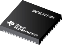
SN65LVCP404 LVDS 4x4 交叉点交换器
 The SN65LVCP404 is a 4x4 non-blocking crosspoint switch in a flow-through pin-out allowing for ease in PCB layout. VML signaling is used to achieve a high-speed data throughput while using low power. Each of the output drivers includes a 4:1 multiplexer to allow any input to be routed to any output. Internal signal paths are fully differential to achieve the high signaling speeds while maintaining low signal skews. The SN65LVCP404 incorporates 100-
 termination resistors for those applications where board space is a premium. Built-in transmit pre-emphasis and receive equalization for superior signal integrity performance.
The SN65LVCP404 is characterized for operation from -40°C to 85°C
|
SN65LVCP202 |
SN65LVCP204 |
SN65LVCP22 |
SN65LVCP23 |
SN65LVCP402 |
SN65LVCP404 |
SN65LVDS122 |
SN65LVDS250 |
| No. of Rx |
2 |
4 |
2 |
2 |
2 |
4 |
2 |
4 |
| No. of Tx |
2 |
4 |
2 |
2 |
2 |
4 |
2 |
4 |
| Signaling Rate(Mbps) |
2500 |
2500 |
1000 |
1300 |
4250 |
4250 |
1500 |
2000 |
| Supply Voltage(s)(V) |
3.3 |
3.3 |
3.3 |
3.3 |
3.3 |
3.3 |
3.3 |
3.3 |
| ICC(Max)(mA) |
115 |
220 |
85 |
65 |
110 |
220 |
100 |
145 |
| Pin/Package |
24VQFN |
48VQFN |
16SOIC, 16TSSOP |
16SOIC, 16TSSOP |
24VQFN |
48VQFN |
16SOIC, 16TSSOP |
38TSSOP |
| Operating Temperature Range(°C) |
-40 to 85 |
-40 to 85 |
-40 to 85 |
-40 to 85 |
-40 to 85 |
-40 to 85 |
-40 to 85 |
-40 to 85 |
| Peak-to-Peak Jitter(Max)(ps) |
30 |
30 |
105 |
100 |
30 |
30 |
65 |
110 |
| Output Signal |
VML |
VML |
LVDS |
LVPECL |
VML |
VML |
LVDS |
LVDS |
| Input Signal |
CML,VML |
CML,VML |
CML, LVDS, LVPECL |
CML, LVDS, LVPECL |
CML,VML |
CML,VML |
CML, LVDS, LVPECL |
CML, LVDS, LVPECL |
| Part-to-Part Skew(Max)(ps) |
300 |
300 |
100 |
100 |
500 |
300 |
100 |
300 |
| Rx tpd(Typ)(ns) |
0.5 |
0.7 |
0.65 |
0.65 |
1 |
0.5 |
0.65 |
0.8 |
| Tx tpd(Typ)(ns) |
0.5 |
0.7 |
0.65 |
0.65 |
1 |
0.5 |
0.65 |
0.8 |
| ESD HBM(kV) |
4 |
3 |
5 |
5 |
3 |
3 |
4 |
3 |
| Approx. Price (US$) |
3.80 | 1ku |
6.00 | 1ku |
2.25 | 1ku |
4.00 | 1ku |
5.80 | 1ku |
9.00 | 1ku |
3.75 | 1ku |
6.75 | 1ku |
SN65LVCP404 特性
- Up to 4.25 Gbps Operation
- Non-blocking Architecture Allows Each Output to be Connected to Any Input
- 30 ps of Deterministic Jitter
- Selectable Transmit Pre-Emphasis Per Lane
- Selectable Receive Equalization
- Available Packaging 48 Pin QFN
- Propagation Delay Times: 500 ps Typical
- Inputs Electrically Compatible With CML Signal Levels
- Operates From a Single 3.3-V Supply
- Ability to 3-STATE ouputs
- Low Power: 560 mW
- Integrated Termination Resistors
- APPLICATIONS
- Clock Buffering/Clock MUXing
- Wireless Base Stations
- High-Speed Network Routing
- Telecom/Datacom
- XAUI 802.3ae Protocol Backplane Redundancy
SN65LVCP404 芯片订购指南
| 器件 |
状态 |
温度 |
价格 |
封装 | 引脚 |
封装数量 | 封装载体 |
丝印标记 |
| SN65LVCP404RGZR |
ACTIVE |
-40 to 85 |
3.80 | 1ku |
VQFN (RGE) | 48 |
3000 | LARGE T&R |
LVCP404 |
| SN65LVCP404RGZT |
ACTIVE |
-40 to 85 |
4.40 | 1ku |
VQFN (RGE) | 48 |
250 | SMALL T&R |
LVCP404 |
SN65LVCP404 质量与无铅数据
| 器件 |
环保计划* |
铅/焊球涂层 |
MSL 等级/回流焊峰 |
环保信息与无铅 (Pb-free) |
DPPM / MTBF / FIT 率 |
| SN65LVCP404RGZR |
Green (RoHS & no Sb/Br) |
CU NIPDAU |
Level-3-260C-168 HR |
SN65LVCP404RGZR |
SN65LVCP404RGZR |
| SN65LVCP404RGZT |
Green (RoHS & no Sb/Br) |
CU NIPDAU |
Level-3-260C-168 HR |
SN65LVCP404RGZT |
SN65LVCP404RGZT |
SN65LVCP404 应用技术支持与电子电路设计开发资源下载
- SN65LVCP404 数据资料 dataSheet 下载.PDF
- TI 德州仪器均衡器和转接驱动器选型与价格 . xls
- 所选封装材料的热学和电学性质 (PDF 645 KB)
- 接口选择指南 (Rev. D) (PDF 2994 KB)
- Signaling Rate vs. Distance for Differential Buffers (PDF 420 KB)
- Q1 2009 Issue Analog Applications Journal (slyt319.PDF, 1.39 MB)
- Isolated RS-485 Reference Design (PDF 80 KB)
- 无铅组件涂层的保存期评估 (PDF 1305 KB)
- Analog Signal Chain Guide (8.62 MB)
- Industrial Interface IC Solutions (101 KB)
SN65LVCP404 TI 工具和软件
 The SN65LVCP404 is a 4x4 non-blocking crosspoint switch in a flow-through pin-out allowing for ease in PCB layout. VML signaling is used to achieve a high-speed data throughput while using low power. Each of the output drivers includes a 4:1 multiplexer to allow any input to be routed to any output. Internal signal paths are fully differential to achieve the high signaling speeds while maintaining low signal skews. The SN65LVCP404 incorporates 100-
![]() termination resistors for those applications where board space is a premium. Built-in transmit pre-emphasis and receive equalization for superior signal integrity performance.
termination resistors for those applications where board space is a premium. Built-in transmit pre-emphasis and receive equalization for superior signal integrity performance.
