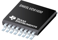
SN65LVDS1050 2.7V 双路 LVDS 发送器/接收器
 The SN65LVDS1050 is similar to the SN65LVDS050 except that it is characterized for operation with a lower supply voltage range and packaged in the thin shrink outline package for portable battery-powered applications.
The differential line drivers and receivers use low-voltage differential signaling (LVDS) to achieve signaling rates as high as 400 Mbps. The drivers provide a minimum differential output voltage magnitude of 247 mV into a 100-![]() load and receipt of 100-mV signals with up to 1 V of ground potential difference between a transmitter and receiver.
load and receipt of 100-mV signals with up to 1 V of ground potential difference between a transmitter and receiver.
The intended application of this device and signaling technique is for point-to-point baseband data transmission over controlled impedance media of approximately 100-![]() characteristic impedance
characteristic impedance
| SN65LVDM050 | SN65LVDM051 | SN65LVDS049 | SN65LVDS050 | SN65LVDS051 | SN65LVDS1050 | SN65LVDS32B | SN65LVDS33 | SN65LVDT32B | SN65LVDT33 | |
| Input Signal | LVDM, LVTTL | LVDM, LVTTL | LVDS, LVTTL | LVDS, LVTTL | LVDS, LVTTL | LVDS, LVTTL | LVDS | CMOS, ECL, LVCMOS, LVDS, LVECL, LVPECL, PECL | LVDS | LVDS, LVECL, LVPECL, PECL |
| Output Signal | LVDM, LVTTL | LVDM, LVTTL | LVDS, LVTTL | LVDS, LVTTL | LVDS, LVTTL | LVDS, LVTTL | LVTTL | LVTTL | LVTTL | LVTTL |
| No. of Rx | 2 | 2 | 2 | 2 | 2 | 2 | 4 | 4 | 4 | 4 |
| No. of Tx | 2 | 2 | 2 | 2 | 2 | 2 | ||||
| Signaling Rate(Mbps) | 500TX/100RX | 500TX/100RX | 400 | 400TX/100RX | 400TX/100RX | 400 | 400 | 400 | 400 | 400 |
| Supply Voltage(s)(V) | 3.3 | 3.3 | 3.3 | 3.3 | 3.3 | 3.3 | 3.3 | 3.3 | 3.3 | 3.3 |
| ICC(Max)(mA) | 27 | 27 | 35 | 20 | 20 | 20 | 23 | 23 | 23 | 23 |
| Rx tpd(Typ)(ns) | 3.7 | 3.7 | 1.9 | 3.7 | 3.7 | 3.7 | 4 | 4 | 4 | 4 |
| Tx tpd(Typ)(ns) | 1.7 | 1.7 | 1.3 | 1.7 | 1.7 | 1.7 | ||||
| Part-to-Part Skew(Max)(ps) | 1000 | 1000 | 1000 | 1000 | 1000 | 1000 | 1000 | |||
| Pin/Package | 16SOIC, 16TSSOP | 16SOIC, 16TSSOP | 16TSSOP | 16SOIC, 16TSSOP | 16SOIC, 16TSSOP | 16TSSOP | 16SOIC | 16SOIC, 16TSSOP | 16SOIC | 16SOIC, 16TSSOP |
| Operating Temperature Range(°C) | -40 to 85 | -40 to 85 | -40 to 85 | -40 to 85 | -40 to 85 | -40 to 85 | -40 to 85 | -40 to 85 | -40 to 85 | -40 to 85 |
| ESD HBM(kV) | 12 | 12 | 10 | 12 | 12 | 12 | 15 | 15 | 15 | 15 |
| Approx. Price (US$) | 1.50 | 1ku | 1.50 | 1ku | 0.95 | 1ku | 1.50 | 1ku | 1.50 | 1ku | 1.65 | 1ku | 2.70 | 1ku | 1.20 | 1ku | 3.40 | 1ku | 1.50 | 1ku |
SN65LVDS1050 特性
- Typically Meets or Exceeds ANSI TIA/EIA-644-1995 Standard
- Operates From a Single 2.4-V to 3.6-V Supply
- Signaling Rates up to 400 Mbit/s
- Bus-Terminal ESD Exceeds 12 kV
- Low-Voltage Differential Signaling With Typical Output Voltages of 285 mV and a 100
 Load
Load
- Propagation Delay Times
- Driver: 1.7 ns Typ
- Receiver: 3.7 ns Typ
- Driver: 25-mW Typical
- Receiver: 60-mW Typical
- Power Dissipation at 200 MHz
- Driver: 25 mW Typical
- Receiver: 60 mW Typical
- LVTTL Input Levels Are 5 V Tolerant
- Receiver Maintains High Input Impedance
- Receiver Has Open-Circuit Fail Safe
- Available in Thin Shink Outline Packaging With 20-mil Lead Pitch
SN65LVDS1050 芯片订购指南
| 器件 | 状态 | 温度 | 价格 | 封装 | 引脚 | 封装数量 | 封装载体 | 丝印标记 |
| SN65LVDS1050PW | ACTIVE | -40 to 85 | 2.00 | 1ku | TSSOP (PW) | 16 | 90 | TUBE | |
| SN65LVDS1050PWG4 | ACTIVE | -40 to 85 | 2.00 | 1ku | TSSOP (PW) | 16 | 90 | TUBE | |
| SN65LVDS1050PWR | ACTIVE | -40 to 85 | 1.65 | 1ku | TSSOP (PW) | 16 | 2000 | LARGE T&R | |
| SN65LVDS1050PWRG4 | ACTIVE | -40 to 85 | 1.65 | 1ku | TSSOP (PW) | 16 | 2000 | LARGE T&R |
SN65LVDS1050 质量与无铅数据
| 器件 | 环保计划* | 铅/焊球涂层 | MSL 等级/回流焊峰 | 环保信息与无铅 (Pb-free) | DPPM / MTBF / FIT 率 |
| SN65LVDS1050PW | Green (RoHS & no Sb/Br) | CU NIPDAU | Level-1-260C-UNLIM | SN65LVDS1050PW | SN65LVDS1050PW |
| SN65LVDS1050PWG4 | Green (RoHS & no Sb/Br) | CU NIPDAU | Level-1-260C-UNLIM | SN65LVDS1050PWG4 | SN65LVDS1050PWG4 |
| SN65LVDS1050PWR | Green (RoHS & no Sb/Br) | CU NIPDAU | Level-1-260C-UNLIM | SN65LVDS1050PWR | SN65LVDS1050PWR |
| SN65LVDS1050PWRG4 | Green (RoHS & no Sb/Br) | CU NIPDAU | Level-1-260C-UNLIM | SN65LVDS1050PWRG4 | SN65LVDS1050PWRG4 |
SN65LVDS1050 应用技术支持与电子电路设计开发资源下载
- SN65LVDS1050 数据资料 dataSheet 下载.PDF
- TI 德州仪器LVDS PHYs选型与价格 . xls
- 所选封装材料的热学和电学性质 (PDF 645 KB)
- 使用数字隔离器设计隔离式 I2C 总线接口 (zhct119.PDF, 339 KB)
- 1Q 2011 Issue Analog Applications Journal (slyt399.PDF, 964 KB)
- 接口选择指南 (Rev. D) (PDF 2994 KB)
- Signaling Rate vs. Distance for Differential Buffers (PDF 420 KB)
- Q1 2009 Issue Analog Applications Journal (slyt319.PDF, 1.39 MB)
- Isolated RS-485 Reference Design (PDF 80 KB)
- 无铅组件涂层的保存期评估 (PDF 1305 KB)
- Analog Signal Chain Guide (8.62 MB)
- Industrial Interface IC Solutions (101 KB)

