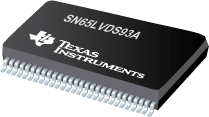
SN65LVDS93A 10MHz - 135MHz LVDS Serdes 发送器
When transmitting, data bits D0 through D27 are each loaded into registers upon the edge of the input clock signal (CLKIN). The rising or falling edge of the clock can be selected via the clock select (CLKSEL) pin. The frequency of CLKIN is multiplied seven times and then used to serially unload the data registers in 7-bit slices
SN65LVDS93A
Number of Parallel Inputs
28
Serial Data Transmitter Channels
4
PLL Frequency(MHz)
10 - 135
ICC(mA)
110
Supply Voltage(s)(V)
3.3
Pin/Package
56TSSOP, 56BGA MICROSTAR JUNIOR
Footprint
DS90CR287
Operating Temperature Range(°C)
-40 to 85
Driver tpd(ns)
14.2
Type of Line Circuit
LVDS
SN65LVDS93A 特性
Industrial Temperature Range –40°C to 85°C
LVDS Display Serdes Interfaces Directly to LCD Display Panels with Integrated LVDS
Package Options: 4.5mm × 7mm BGA, and 8.1mm × 14mm TSSOP
1.8V up to 3.3V Tolerant Data Inputs to Connect Directly to Low-Power, Low-Voltage Application and Graphic Processors
Transfer Rate up to 135Mpps (Mega Pixel Per Second); Pixel Clock Frequency Range 10MHz to 135MHz
Suited for Display Resolutions Ranging From HVGA up to HD With Low EMI
Operates From a Single 3.3V Supply and 170mW (typ.) at 75MHz
28 Data Channels Plus Clock In Low-Voltage TTL to 4 Data Channels Plus Clock Out Low-Voltage Differential
Consumes Less Than 1mW When Disabled
Selectable Rising or Falling Clock Edge Triggered Inputs
ESD: 5kV HBM
Support Spread Spectrum Clocking (SSC)
Compatible with all OMAP2x, OMAP™3x, and DaVinci Application Processors
APPLICATIONS
LCD Display Panel Driver
UMPC and Netbook PC
Digital Picture Frame
SN65LVDS93A 芯片订购指南
器件
状态
温度
价格
封装 | 引脚
封装数量 | 封装载体
丝印标记
SN65LVDS93ADGG
ACTIVE
-40 to 85
5.35 | 1ku
TSSOP (DGG) | 56 35 | TUBE
SN65LVDS93ADGGR
ACTIVE
-40 to 85
4.45 | 1ku
TSSOP (DGG) | 56 2000 | LARGE T&R
SN65LVDS93A 质量与无铅数据
器件
环保计划*
铅/焊球涂层
MSL 等级/回流焊峰
环保信息与无铅 (Pb-free)
DPPM / MTBF / FIT 率
SN65LVDS93ADGG
Green (RoHS & no Sb/Br)
CU NIPDAU
Level-2-260C-1 YEAR
SN65LVDS93ADGG
SN65LVDS93ADGG
SN65LVDS93ADGGR
Green (RoHS & no Sb/Br)
CU NIPDAU
Level-2-260C-1 YEAR
SN65LVDS93ADGGR
SN65LVDS93ADGGR
SN65LVDS93A 应用技术支持与电子电路设计开发资源下载
SN65LVDS93A 数据资料 dataSheet 下载 .PDF TI 德州仪器FlatLink选型与价格 . xls 所选封装材料的热学和电学性质 (PDF 645 KB)Q1 2009 Issue Analog Applications Journal (slyt319.PDF, 1.39 MB)使用 TI 的 SN65LVDS93A 收发器改善 CAN 网络安全性 (zhct033.PDF, 299 KB)Isolated CAN Reference Design (PDF 48 KB)Isolated RS-485 Reference Design (PDF 80 KB)无铅组件涂层的保存期评估 (PDF 1305 KB)Isolated CAN EVM User's Guide (PDF 1168 KB)Energy Harvesting: Solar Solutions Guide (PDF 409 KB)Analog Signal Chain Guide (8.62 MB)Industrial Interface IC Solutions (101 KB)
SN65LVDS93A 工具与软件
培训内容
型号
软件/工具类型
通过 CAN 总线进行工业控制的演示平台
CANBUS-DEMO 硬件参考设计
 The SN65LVDS93A LVDS serdes (serializer/deserializer) transmitter contains four 7-bit parallel load serial-out shift registers, a 7 × clock synthesizer, and five low-voltage differential signaling (LVDS) drivers in a single integrated circuit. These functions allow 28 bits of single-ended LVTTL data to be synchronously transmitted over five balanced-pair conductors for receipt by a compatible receiver, such as the SN65LVDS94.
