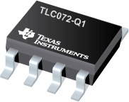
TLC072-Q1 汽车类双路宽带高输出驱动运算放大器
 The first members of TI’s new BiMOS general-purpose operational amplifier family are the TLC07x. The BiMOS family concept is simple: provide an upgrade path for BiFET users who are moving away from dual-supply to single-supply systems and demand higher AC and dc performance. With performance rated from 4.5 V to 16 V across commercial (0°C to 70°C) and an extended industrial temperature range (–40°C to 125°C), BiMOS suits a wide range of audio, automotive, industrial and instrumentation applications. Familiar features like offset nulling pins enable higher levels of performance in a variety of applications.
Developed in TI’s patented LBC3 BiCMOS process, the new BiMOS amplifiers combine a very high input impedance low-noise CMOS front end with a high-drive bipolar output stage, thus providing the optimum performance features of both. AC performance improvements over the TL07x BiFET predecessors include a bandwidth of 10 MHz (an increase of 300%) and voltage noise of 7 nV/ Hz (an improvement of 60%). DC improvements include a factor of 4 reduction in input offset voltage down to 1.5 mV (maximum) in the standard grade, and a power supply rejection improvement of greater than 40 dB to 130 dB. Added to this list of impressive features is the ability to drive ±50-mA loads comfortably from an ultrasmall-footprint MSOP PowerPAD™ package, which positions the TLC07x as the ideal high-performance general-purpose operational amplifier family
�
|
TLC072-Q1 |
| Number of Channels |
2 |
| GBW(Typ)(MHz) |
10 |
| Offset Drift(Typ)(uV/C) |
1.2 |
| IIB(Max)(pA) |
50 |
| CMRR(Min)(dB) |
80 |
| Rating |
Automotive |
| Pin/Package |
8SOIC |
| Operating Temperature Range(C) |
-40 to 125 |
| Approx. Price (US$) |
0.80 | 1ku |
TLC072-Q1 特性
- Qualified for Automotive Applications
- Wide Bandwidth . . . 10 MHz
- High-Output Drive
- IOH . . . 57 mA at VDD – 1.5 V
- IOL . . . 55 mA at 0.5 V
- High Slew Rate
- SR+ . . . 16 V/µs
- SR– . . . 19 V/µs
- Wide Supply Range . . . 4.5 V to 16 V
- Supply Current . . . 1.9 mA/Channel
- Ultralow Power Shutdown Mode IDD . . . 125 mA/Channel
- Low Input Noise Voltage . . . 7 nV/Hz
- Input Offset Voltage . . . 60 µV
- Small 8-Pin SOIC Package
TLC072-Q1 芯片订购指南
| 器件 |
状态 |
温度 |
价格(美元) |
封装 | 引脚 |
封装数量 | 封装载体 |
丝印标记 |
| TLC072QDRQ1 |
ACTIVE |
-40 to 125 |
0.80 | 1ku |
SOIC (D) | 8 |
2500 |
|
TLC072-Q1 质量与无铅数据
| 器件 |
环保计划* |
铅/焊球涂层 |
MSL 等级/回流焊峰 |
环保信息与无铅 (Pb-free) |
DPPM / MTBF / FIT 率 |
| TLC072QDRQ1 |
Green (RoHS & no Sb/Br) |
CU NIPDAU |
Level-1-260C-UNLIM |
TLC072QDRQ1 |
TLC072QDRQ1 |
TLC072-Q1 应用技术支持与电子电路设计开发资源下载
- TLC072-Q1 数据资料 dataSheet 下载.PDF
- TI 德州仪器仪运算放大器 (Op Amp)产品选型与价格 . xls
- 所选封装材料的热学和电学性质 (PDF 645 KB)
- 高速数据转换 (PDF 1967 KB)
- 在 PSPICE 中使用德州仪器 (TI) SPICE 模型 (zhca088.HTM, 8 KB)
- PowerPAD™ Thermally Enhanced Package (slma002g.HTM, 8 KB)
- 运算放大器的单电源操作 (PDF 2174 KB)
- Tuning in Amplifiers (PDF 44 KB)
- Op Amp Performance Analysis (PDF 76 KB)
- An Error Analysis of the ISO102 in a Small Signal Measuring Application (PDF 29 KB)
- Level Shifting Signals with Differential Amplifiers (PDF 23 KB)
- Operational Amplifier Macromodels: A Comparison (PDF 59 KB)
 The first members of TI’s new BiMOS general-purpose operational amplifier family are the TLC07x. The BiMOS family concept is simple: provide an upgrade path for BiFET users who are moving away from dual-supply to single-supply systems and demand higher AC and dc performance. With performance rated from 4.5 V to 16 V across commercial (0°C to 70°C) and an extended industrial temperature range (–40°C to 125°C), BiMOS suits a wide range of audio, automotive, industrial and instrumentation applications. Familiar features like offset nulling pins enable higher levels of performance in a variety of applications.
 Hz (an improvement of 60%). DC improvements include a factor of 4 reduction in input offset voltage down to 1.5 mV (maximum) in the standard grade, and a power supply rejection improvement of greater than 40 dB to 130 dB. Added to this list of impressive features is the ability to drive ±50-mA loads comfortably from an ultrasmall-footprint MSOP PowerPAD™ package, which positions the TLC07x as the ideal high-performance general-purpose operational amplifier family