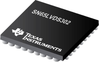
SN65LVDS302 可编程 27 位显示屏串行接口发送器
 The SN65LVDS302 receiver de-serializes FlatLink™3G compliant serial input data to 27 parallel data outputs. The SN65LVDS302 receiver contains one shift register to load 30 bits from 1, 2 or 3 serial inputs and latches the 24 pixel bits and 3 control bits out to the parallel CMOS outputs after checking the parity bit. If the parity check confirms correct parity, the Channel Parity Error (CPE) output remains low. If a parity error is detected, the CPE output generates a high pulse while the data output bus disregards the newly-received pixel. Instead, the last data word is held on the output bus for another clock cycle.
The serial data and clock are received via Sub Low-Voltage Differential Signalling (SubLVDS) lines
|
SN65LVDS301 |
SN65LVDS302 |
SN65LVDS303 |
SN65LVDS304 |
SN65LVDS305 |
SN65LVDS306 |
SN65LVDS311 |
| Number of Parallel Outputs |
|
27 |
|
27 |
|
27 |
|
| Number of Parallel Inputs |
27 |
|
27 |
|
27 |
|
27 |
| Data Throughput(MB/s) |
1755 |
1755 |
810 |
810 |
405 |
405 |
1755 |
| Serial Data Receiver Channels |
|
3 |
|
2 |
|
1 |
|
| Serial Data Transmitter Channels |
3 |
|
2 |
|
1 |
|
3 |
| Type of Line Circuit |
subLVDS |
subLVDS |
subLVDS |
subLVDS |
subLVDS |
subLVDS |
subLVDS |
| Supply Voltage(s)(V) |
1.8 |
1.8 |
1.8 |
1.8 |
1.8 |
1.8 |
1.8 |
| PLL Frequency(MHz) |
4 - 65 |
4 - 65 |
4 - 30 |
4 - 30 |
4 - 15 |
4 - 15 |
4 - 65 |
| Footprint |
SN65LVDS301 |
SN65LVDS302 |
SN65LVDS301 |
SN65LVDS302 |
SN65LVDS301 |
SN65LVDS302 |
SN65LVDS311 |
| Operating Temperature Range(°C) |
-40 to 85 |
-40 to 85 |
-40 to 85 |
-40 to 85 |
-40 to 85 |
-40 to 85 |
-40 to 85 |
| Pin/Package |
80BGA MICROSTAR JUNIOR |
80BGA MICROSTAR JUNIOR |
80BGA MICROSTAR JUNIOR |
80BGA MICROSTAR JUNIOR |
80BGA MICROSTAR JUNIOR |
80BGA MICROSTAR JUNIOR |
49DSBGA |
SN65LVDS302 特性
- Serial Interface Technology
- Compatible with FlatLink™3G such as SN65LVDS301
- Supports Video Interfaces up to 24-bit RGB Data and 3 Control Bits Received over 1, 2 or 3 SubLVDS Differential Lines
- SubLVDS Differential Voltage Levels
- Up to 1.755 Gbps Data Throughput
- Three Operating Modes to Conserve Power
- Active mode QVGA - 17 mW
- Typical Shutdown - 0.7 µW
- TypicalStandby Mode - 27 µW Typical
- Bus-Swap Function for PCB-Layout Flexibility
- ESD Rating > 4 kV (HBM)
- Pixel Clock Range of 4 MHz-65 MHz
- Failsafe on all CMOS Inputs
- Packaged in 5 mm x 5 mm MicroStar Junior µBGA® with 0,5 mm Ball Pitch
- Very low EMI meets SAE J1752/3 'Kh'-spec
- APPLICATIONS
- Small Low-Emission Interface between Graphics Controller and LCD Display
- Mobile Phones & Smart Phones
- Portable Multimedia Players
SN65LVDS302 芯片订购指南
SN65LVDS302 质量与无铅数据
| 器件 |
环保计划* |
铅/焊球涂层 |
MSL 等级/回流焊峰 |
环保信息与无铅 (Pb-free) |
DPPM / MTBF / FIT 率 |
| SN65LVDS302ZQE |
Green (RoHS & no Sb/Br) |
SNAGCU |
Level-3-260C-168 HR |
SN65LVDS302ZQE |
SN65LVDS302ZQE |
| SN65LVDS302ZQER |
Green (RoHS & no Sb/Br) |
SNAGCU |
Level-3-260C-168 HR |
SN65LVDS302ZQER |
SN65LVDS302ZQER |
SN65LVDS302 应用技术支持与电子电路设计开发资源下载
- SN65LVDS302 数据资料 dataSheet 下载.PDF
- TI 德州仪器FlatLink选型与价格 . xls
- 所选封装材料的热学和电学性质 (PDF 645 KB)
- Q1 2009 Issue Analog Applications Journal (slyt319.PDF, 1.39 MB)
- 使用 TI 的 SN65LVDS302 收发器改善 CAN 网络安全性 (zhct033.PDF, 299 KB)
- Isolated CAN Reference Design (PDF 48 KB)
- Isolated RS-485 Reference Design (PDF 80 KB)
- 无铅组件涂层的保存期评估 (PDF 1305 KB)
- Isolated CAN EVM User's Guide (PDF 1168 KB)
- Energy Harvesting: Solar Solutions Guide (PDF 409 KB)
- Analog Signal Chain Guide (8.62 MB)
- Industrial Interface IC Solutions (101 KB)
 The SN65LVDS302 receiver de-serializes FlatLink™3G compliant serial input data to 27 parallel data outputs. The SN65LVDS302 receiver contains one shift register to load 30 bits from 1, 2 or 3 serial inputs and latches the 24 pixel bits and 3 control bits out to the parallel CMOS outputs after checking the parity bit. If the parity check confirms correct parity, the Channel Parity Error (CPE) output remains low. If a parity error is detected, the CPE output generates a high pulse while the data output bus disregards the newly-received pixel. Instead, the last data word is held on the output bus for another clock cycle.
