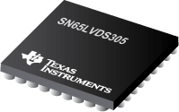
SN65LVDS305 可编程 27 位显示屏串行接口发送器
 The SN65LVDS305 serializer device converts 27 parallel data inputs to one sub-low-voltage differential signaling (SubLVDS) serial output. It loads a shift register with 24 pixel bits and 3 control bits from the parallel CMOS input interface. In addition to the 27 data bits, the device adds a parity bit and two reserved bits into a 30-bit data word. Each word is latched into the device by the pixel clock (PCLK). The parity bit (odd parity) allows a receiver to detect single bit errors. The serial shift register is uploaded at 30 times the pixel-clock data rate. A copy of the pixel clock is output on a separate differential output.
FPC cabling typically interconnects the SN65LVDS305 with the display. Compared to parallel signaling, the SN65LVDS305 outputs reduce the EMI of the interconnect by over 20 dB
|
SN65LVDS301 |
SN65LVDS302 |
SN65LVDS303 |
SN65LVDS304 |
SN65LVDS305 |
SN65LVDS306 |
SN65LVDS311 |
| Number of Parallel Outputs |
|
27 |
|
27 |
|
27 |
|
| Number of Parallel Inputs |
27 |
|
27 |
|
27 |
|
27 |
| Data Throughput(MB/s) |
1755 |
1755 |
810 |
810 |
405 |
405 |
1755 |
| Serial Data Receiver Channels |
|
3 |
|
2 |
|
1 |
|
| Serial Data Transmitter Channels |
3 |
|
2 |
|
1 |
|
3 |
| Type of Line Circuit |
subLVDS |
subLVDS |
subLVDS |
subLVDS |
subLVDS |
subLVDS |
subLVDS |
| Supply Voltage(s)(V) |
1.8 |
1.8 |
1.8 |
1.8 |
1.8 |
1.8 |
1.8 |
| PLL Frequency(MHz) |
4 - 65 |
4 - 65 |
4 - 30 |
4 - 30 |
4 - 15 |
4 - 15 |
4 - 65 |
| Footprint |
SN65LVDS301 |
SN65LVDS302 |
SN65LVDS301 |
SN65LVDS302 |
SN65LVDS301 |
SN65LVDS302 |
SN65LVDS311 |
| Operating Temperature Range(°C) |
-40 to 85 |
-40 to 85 |
-40 to 85 |
-40 to 85 |
-40 to 85 |
-40 to 85 |
-40 to 85 |
| Pin/Package |
80BGA MICROSTAR JUNIOR |
80BGA MICROSTAR JUNIOR |
80BGA MICROSTAR JUNIOR |
80BGA MICROSTAR JUNIOR |
80BGA MICROSTAR JUNIOR |
80BGA MICROSTAR JUNIOR |
49DSBGA |
SN65LVDS305 特性
- FlatLink™3G Serial-Interface Technology
- Compatible With FlatLink3G Receivers Such as SN65LVDS306
- Input Supports 24-bit RGB Video Mode Interface
- 24-Bit RGB Data, 3 Control Bits, 1 Parity Bit, and 2 Reserved Bits Transmitted Over One Differential Line
- SubLVDS Differential Voltage Levels
- Effective Data Throughput up to 405 Mbps
- Three Operating Modes to Conserve Power
- Active-Mode QVGA 17.4 mW (Typical)
- Shutdown Mode
 0.5 µA (Typical)
- Bus Swap for Increased PCB Layout Flexibility
- 1.8-V Supply Voltage
- ESD Rating > 2 kV (HBM)
- Typical Application: Host-Controller to Display-Module Interface
- Pixel Clock Range of 4 MHz-15 MHz
- Failsafe on all CMOS Inputs
- Packaging: 80-Terminal 5-mm × 5-mm µBGA®
SN65LVDS305 芯片订购指南
SN65LVDS305 质量与无铅数据
| 器件 |
环保计划* |
铅/焊球涂层 |
MSL 等级/回流焊峰 |
环保信息与无铅 (Pb-free) |
DPPM / MTBF / FIT 率 |
| SN65LVDS305ZQE |
Green (RoHS & no Sb/Br) |
SNAGCU |
Level-3-260C-168 HR |
SN65LVDS305ZQE |
SN65LVDS305ZQE |
| SN65LVDS305ZQER |
Green (RoHS & no Sb/Br) |
SNAGCU |
Level-3-260C-168 HR |
SN65LVDS305ZQER |
SN65LVDS305ZQER |
SN65LVDS305 应用技术支持与电子电路设计开发资源下载
- SN65LVDS305 数据资料 dataSheet 下载.PDF
- TI 德州仪器FlatLink选型与价格 . xls
- 所选封装材料的热学和电学性质 (PDF 645 KB)
- Q1 2009 Issue Analog Applications Journal (slyt319.PDF, 1.39 MB)
- 使用 TI 的 SN65LVDS305 收发器改善 CAN 网络安全性 (zhct033.PDF, 299 KB)
- Isolated CAN Reference Design (PDF 48 KB)
- Isolated RS-485 Reference Design (PDF 80 KB)
- 无铅组件涂层的保存期评估 (PDF 1305 KB)
- Isolated CAN EVM User's Guide (PDF 1168 KB)
- Energy Harvesting: Solar Solutions Guide (PDF 409 KB)
- Analog Signal Chain Guide (8.62 MB)
- Industrial Interface IC Solutions (101 KB)
 The SN65LVDS305 serializer device converts 27 parallel data inputs to one sub-low-voltage differential signaling (SubLVDS) serial output. It loads a shift register with 24 pixel bits and 3 control bits from the parallel CMOS input interface. In addition to the 27 data bits, the device adds a parity bit and two reserved bits into a 30-bit data word. Each word is latched into the device by the pixel clock (PCLK). The parity bit (odd parity) allows a receiver to detect single bit errors. The serial shift register is uploaded at 30 times the pixel-clock data rate. A copy of the pixel clock is output on a separate differential output.
 0.5 µA (Typical)
