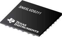
SN65LVDS311 可编程 27 位显示屏串行接口发送器
 The SN65LVDS311 serializer transmits 27 parallel input data over 1, 2, or 3 serial output links. The device pinout is optimized to interface with the OMAP3630 application processor. The device loads a shift register with the 24 pixel bits and 3 control bits from the parallel CMOS input interface. The data are latched into the device by the pixel clock, PCLK. In addition to the 27 bits, the device adds a parity bit and two reserved bits for a total number of 30 serial bits. The parity bit allows a receiver to detect single-bit errors. Odd parity is implemented.
The serial shift register is uploaded through 1, 2, or 3 serial outputs at 30, 15, or 10 times the pixel clock data rate. A copy of the pixel clock is output on an additional differential output
|
SN65LVDS301 |
SN65LVDS302 |
SN65LVDS303 |
SN65LVDS304 |
SN65LVDS305 |
SN65LVDS306 |
SN65LVDS311 |
| Number of Parallel Outputs |
|
27 |
|
27 |
|
27 |
|
| Number of Parallel Inputs |
27 |
|
27 |
|
27 |
|
27 |
| Data Throughput(MB/s) |
1755 |
1755 |
810 |
810 |
405 |
405 |
1755 |
| Serial Data Receiver Channels |
|
3 |
|
2 |
|
1 |
|
| Serial Data Transmitter Channels |
3 |
|
2 |
|
1 |
|
3 |
| Type of Line Circuit |
subLVDS |
subLVDS |
subLVDS |
subLVDS |
subLVDS |
subLVDS |
subLVDS |
| Supply Voltage(s)(V) |
1.8 |
1.8 |
1.8 |
1.8 |
1.8 |
1.8 |
1.8 |
| PLL Frequency(MHz) |
4 - 65 |
4 - 65 |
4 - 30 |
4 - 30 |
4 - 15 |
4 - 15 |
4 - 65 |
| Footprint |
SN65LVDS301 |
SN65LVDS302 |
SN65LVDS301 |
SN65LVDS302 |
SN65LVDS301 |
SN65LVDS302 |
SN65LVDS311 |
| Operating Temperature Range(°C) |
-40 to 85 |
-40 to 85 |
-40 to 85 |
-40 to 85 |
-40 to 85 |
-40 to 85 |
-40 to 85 |
| Pin/Package |
80BGA MICROSTAR JUNIOR |
80BGA MICROSTAR JUNIOR |
80BGA MICROSTAR JUNIOR |
80BGA MICROSTAR JUNIOR |
80BGA MICROSTAR JUNIOR |
80BGA MICROSTAR JUNIOR |
49DSBGA |
SN65LVDS311 特性
- 2.8 × 2.8mm package size
- 1.8V input signal swing
- 24-Bit RGB Data, 3 Control Bits, 1 Parity Bit and 2 Reserved Bits
Transmitted over 1, 2 or 3 Differential Lines
- SubLVDS Differential Voltage Levels
- Three Operating Modes to Conserve Power
- Active-Mode QVGA 17.4mW (typ)
- Active-Mode VGA 28.8mW (typ)
- Shutdown Mode
 0.5µ (typ)
- Standby Mode
 0.5µA (typ)
- ESD Rating > 3kV (HBM)
- Pixel Clock Range of 4MHz–65MHz
- Failsafe on all CMOS Inputs
- Typical Application: Smartphone
SN65LVDS311 芯片订购指南
| 器件 |
状态 |
温度 |
价格 |
封装 | 引脚 |
封装数量 | 封装载体 |
丝印标记 |
| SN65LVDS311YFFR |
ACTIVE |
-40 to 85 |
2.10 | 1ku |
DSBGA (YFF) | 49 |
3000 | LARGE T&R |
|
| SN65LVDS311YFFT |
ACTIVE |
-40 to 85 |
2.45 | 1ku |
DSBGA (YFF) | 49 |
250 | SMALL T&R |
|
SN65LVDS311 质量与无铅数据
| 器件 |
环保计划* |
铅/焊球涂层 |
MSL 等级/回流焊峰 |
环保信息与无铅 (Pb-free) |
DPPM / MTBF / FIT 率 |
| SN65LVDS311YFFR |
Green (RoHS & no Sb/Br) |
SNAGCU |
Level-1-260C-UNLIM |
SN65LVDS311YFFR |
SN65LVDS311YFFR |
| SN65LVDS311YFFT |
Green (RoHS & no Sb/Br) |
SNAGCU |
Level-1-260C-UNLIM |
SN65LVDS311YFFT |
SN65LVDS311YFFT |
SN65LVDS311 应用技术支持与电子电路设计开发资源下载
- SN65LVDS311 数据资料 dataSheet 下载.PDF
- TI 德州仪器FlatLink选型与价格 . xls
- 所选封装材料的热学和电学性质 (PDF 645 KB)
- Q1 2009 Issue Analog Applications Journal (slyt319.PDF, 1.39 MB)
- 使用 TI 的 SN65LVDS311 收发器改善 CAN 网络安全性 (zhct033.PDF, 299 KB)
- Isolated CAN Reference Design (PDF 48 KB)
- Isolated RS-485 Reference Design (PDF 80 KB)
- 无铅组件涂层的保存期评估 (PDF 1305 KB)
- Isolated CAN EVM User's Guide (PDF 1168 KB)
- Energy Harvesting: Solar Solutions Guide (PDF 409 KB)
- Analog Signal Chain Guide (8.62 MB)
- Industrial Interface IC Solutions (101 KB)
 The SN65LVDS311 serializer transmits 27 parallel input data over 1, 2, or 3 serial output links. The device pinout is optimized to interface with the OMAP3630 application processor. The device loads a shift register with the 24 pixel bits and 3 control bits from the parallel CMOS input interface. The data are latched into the device by the pixel clock, PCLK. In addition to the 27 bits, the device adds a parity bit and two reserved bits for a total number of 30 serial bits. The parity bit allows a receiver to detect single-bit errors. Odd parity is implemented.
 0.5µ (typ)
 0.5µA (typ)
